
READ and WRITE operation of 6-T SRAM cell
Static Random Access Memory, sometimes known as SRAM, is a type of semiconductor memory frequently employed in electronic, microprocessor, and general computing applications. Although SRAM memory does not require dynamic refresh, it is nonetheless volatile, which means that when the power is cut off to the memory device, the data is not retained and will vanish.
Because SRAM does not require periodic refreshment while DRAM does, has the advantage of providing greater performance. SRAM sizes are orders of magnitude less than DRAM, however, SRAM is more expensive and less dense than DRAM.
6-T SRAM cell Read Operation
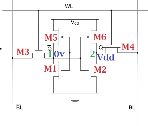
- Assume that node 1 has logic 0v
- So M1 and M6 are ON while M5 and M2 are OFF. Because of this, Node1 = 0V and V2 = VDD.
- Data lines are pre-changed from 0 to VDD and the word line is activated.
- So M3 and M4 are switched ON.
- Since the drain and source for M4 are at the same potential, no current flows in this area.
- However, the drain and source at M3 in LHS have a high differential potential, therefore M3 experiences non-zero current flow.
- Path: M3, M1, and GND
- The voltage at BL starts to decline, which causes the capacitor to discharge and raise V1.
- Since V1 is increasing from 0V and it may turn on M2 if M1 size is small, So for reading operation, M1 should be greater than M3
6-T SRAM cell Write Operation
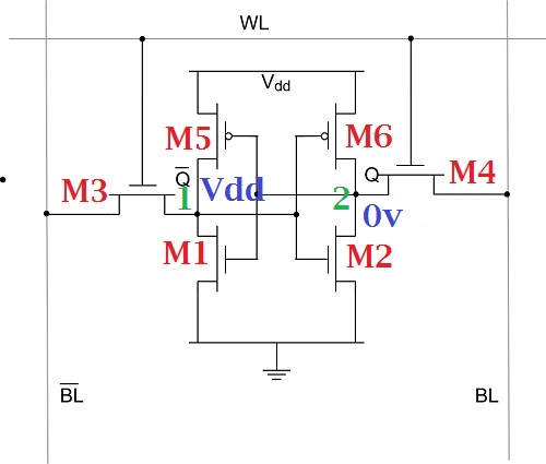
- Consider that Node 1 stores Assume 1.
- So M2 and M5 are ON while M1 and M6 are OFF.
- Prior to the ON state of M2 and M4, V1 = VDD and V2 = 0V.
- As Wordline goes high, M3 and M4 are turned ON.
- Since Node2 < VT1, Node2 cannot be used to turn ON M1. We need to turn ON M1 so that path is created from Node1 to GND and the voltage at Node1 will decrease to zero since the path is pulled down to GND.
- Therefore we turn OFF M2. Node1 < VT2 to turn OFF M2. When Node1 = Vin; M3 goes in the linear region and M5 in the saturation region.
- For a successful Write operation, we should have M4> M6.
SRAM Advantage
The four-transistor SRAM computer memory cell offers certain benefits in terms of density, but this comes at the expense of manufacturing complexity since resistors must be produced, which necessitates additional processing. To match the demands of the cell, the resistors must also have compact dimensions and high values. The lower static power is the six-transistor SRAM circuit’s key benefit. The pull-down resistors in the four transistor variants always have current flowing through them, which raises the chip’s overall power consumption. Due to higher power dissipation, this may restrict the amount of integration as well as aggravate circuit design problems.
SRAM Memory Applications
Microcontrollers frequently use SRAM when simpler operations and low power consumption are required. Additionally, microcontrollers typically do not require the larger memory capacity of DRAM.SRAM memory is employed in applications where speed or low power consumption are priorities as a result of these parameters. It can also be utilized in semiconductor memory applications that require high-capacity memory, such as the working memory in computers, because to its higher density and simpler structure.
In the field of embedded computing, microcontrollers with battery-backed, nonvolatile SRAM are frequently employed. Nonvolatile SRAM technology, unlike Flash memory or EEPROM technology, has no write constraints, or restrictions on the number of write/read cycles, making it perfect for real-time data logging applications.
Transistor Sizing for SRAM
- For Read operation, M1 should be greater than the M3 transistor.
- For the Write operation, the M4 should be greater than the M6 transistor.