
Adjust the CMOS inverter to either reduced leakage or decrease delay by following ways,
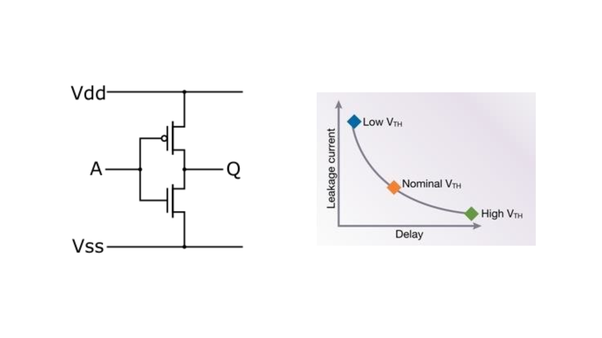
Reducing Leakage Current
I recommend utilizing a larger PMOS (p-channel metal-oxide-semiconductor) transistor along with a smaller NMOS (n-channel metal-oxide-semiconductor) transistor. This approach helps us minimize the sub-threshold leakage current, as we know that PMOS transistors generally exhibit lower leakage compared to NMOS transistors. You’ll find that this strategy can significantly improve the overall efficiency of your circuit design.
Decreasing Delay
Reduce the sizes of both the PMOS and NMOS transistors to decrease the channel resistance and improve the switching speed. This can be achieved by adjusting the width-to-length ratio of the transistors. Utilize high-performance CMOS processes that offer faster transistor switching speeds and reduced parasitic capacitance.
How You Can Fix Setup Violations in Your Design
When we see a setup violation in the design, it means that the delay in a combinational path is more than what is allowed. To fix this, you or I can reduce the delay by upsizing the cells. This step lowers the resistance, which then decreases the RC delay in that path.
How We Define Propagation Delay, Rise Time, and Fall Time
We define propagation delay as the time between the 50% level of the input and the matching 50% level of the output. You and I also measure rise and fall times as the time it takes for the output voltage to shift from 10% to 90% (or the reverse).