
Vias
Via is a connection between two metals. More than one vias should use for metal-to-metal connections.
More vias have offered less resistance. So putting more vias is a better idea.
Imagine there is a metal 2 layer carrying 200uA of current which has to be connected to the source or drain of a transistor. Let’s say, you put a single via and single contact. This will usually have a size of around 0.2×0.2 ie 0.4um²… So this actually means the 200uA of current has to reach the diffusion regions of the transistor through this small region only so we can say that it’s a very bad idea to put single small vias.
Large vias are better or putting two smaller vias are better?
A Large via will provide great stress to the metal layer below. Hence it is always advisable to have multiple smaller vias rather than going in for one large via.
we use multiple vias to increase the reliability/yield of the design at the time of fabrication the larger the number of vias lesser is the resistivity.
Why contact and via have an exact size?
For technologies 0.28um and smaller, the contact and Via sizes are usually exact. This is because of the process. The process itself may vary the contact size but only by about +/-0.05um. This is due to the way global planarization (CMP) is used for inter-metal dielectrics and the formation of contact via tungsten plugs.
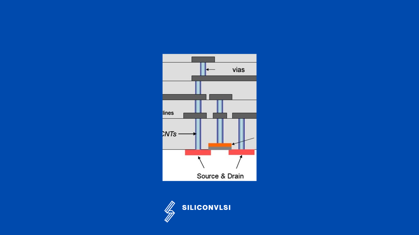
What is the difference between contact and Via?
Contact is used to create a connection between M1 and the poly or M1 and OD. Vias are used for connections between metal layers.
For example, VIA12 for connection between M1 and M2. VIA23 for connection between M2 and M3.
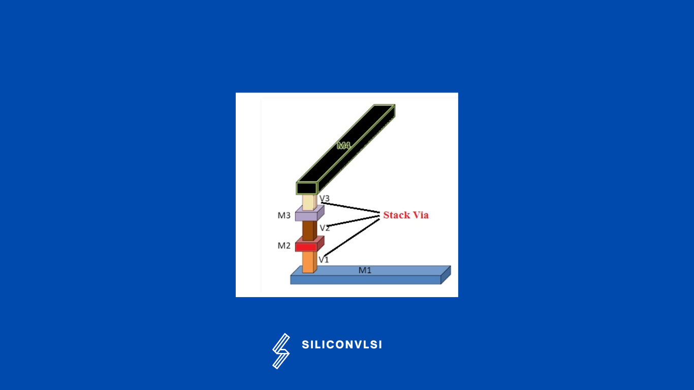
What is Stack Via?
When we place two vias above the others, it’s called stack vias. This type of via has great reliability.
What is the difference between via and contact?
A contact is a connection to the source, drain, and poly, while a via is used to connect two metal layers.