MOSFET ID vs. VGS characteristic
The output characteristics are a graph of drain current ID versus drain to source voltage VDS for different values of the gate to source voltage VGS.
What is Threshold Voltage
The threshold voltage of the NMOS denoted as VTN, is defined2 as the applied gate voltage needed to create an inversion charge under the channel in the semiconductor substrate. In simple terms, we can think of the threshold voltage as the gate voltage required to “turn on” the transistor. For the n-channel enhancement-mode MOSFET, the threshold voltage is positive because a positive gate voltage is required to create the inversion charge. For the p-channel enhancement-mode MOSFET, the threshold voltage is negative because a negative gate voltage is required to create the inversion charge. To understand this, Let’s take the example 0f an NMOS device.
n-channel enhancement-mode MOSFET
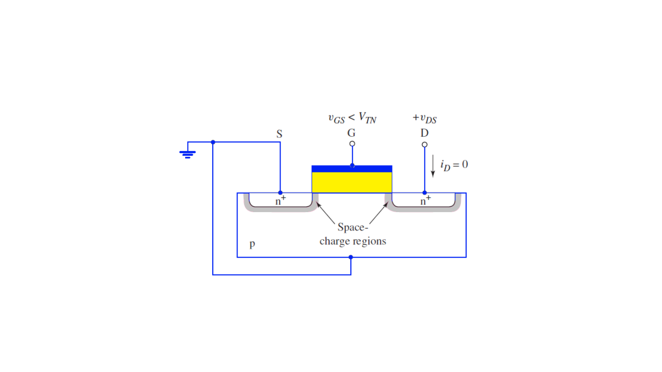
Figure 1 shows an n-channel enhancement-mode MOSFET with the source and substrate terminals connected to the zero. When the Gate to source voltage is less than the threshold voltage, there is no current flow from the channel, it’s called a cut-off region. With this bias configuration, there is no electron inversion layer, the drain-to-substrate PN junction is reverse biased, and the drain current is zero. here please take note that we are neglecting PN junction leakage currents.
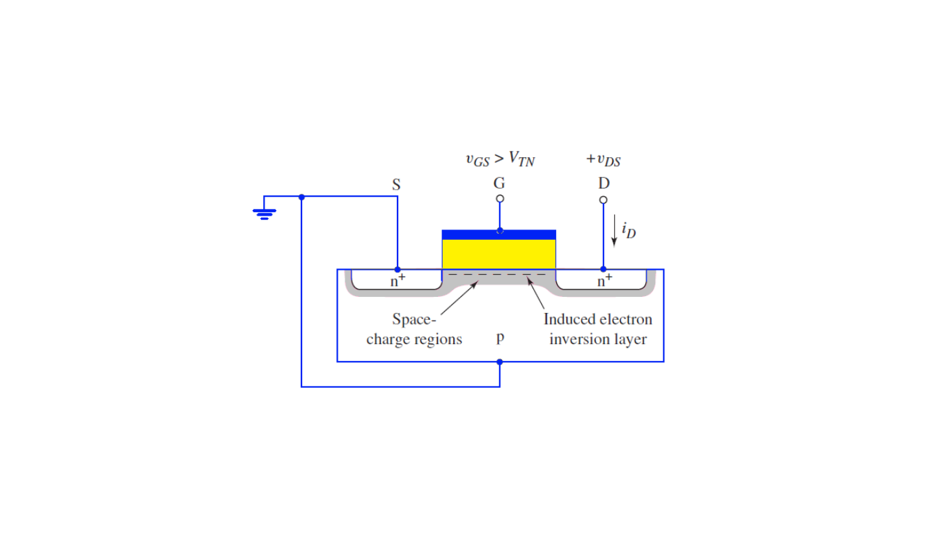
Now if we increase the gate voltage, Figure 2 shows the same MOSFET with an applied gate voltage greater than the threshold voltage. In this situation, an electron inversion layer is created, and, when a small drain voltage is applied, electrons in the inversion layer flow from the
source to the drain terminal. Note that a positive drain voltage creates a reverse-biased drain-to-substrate PN junction, so current flows through the channel region and not through a PN junction.
The ID versus VDS characteristics for small values of VGS is shown in Following Figure 3. When VGS < VTN, the drain current is zero. When VGS is greater than VTN, the channel will form and the inversion charge is formed, and the drain current increases with VDS. Then, with a larger gate voltage, a larger inversion charge density is created, and the drain current will increase for a given value of VDS.
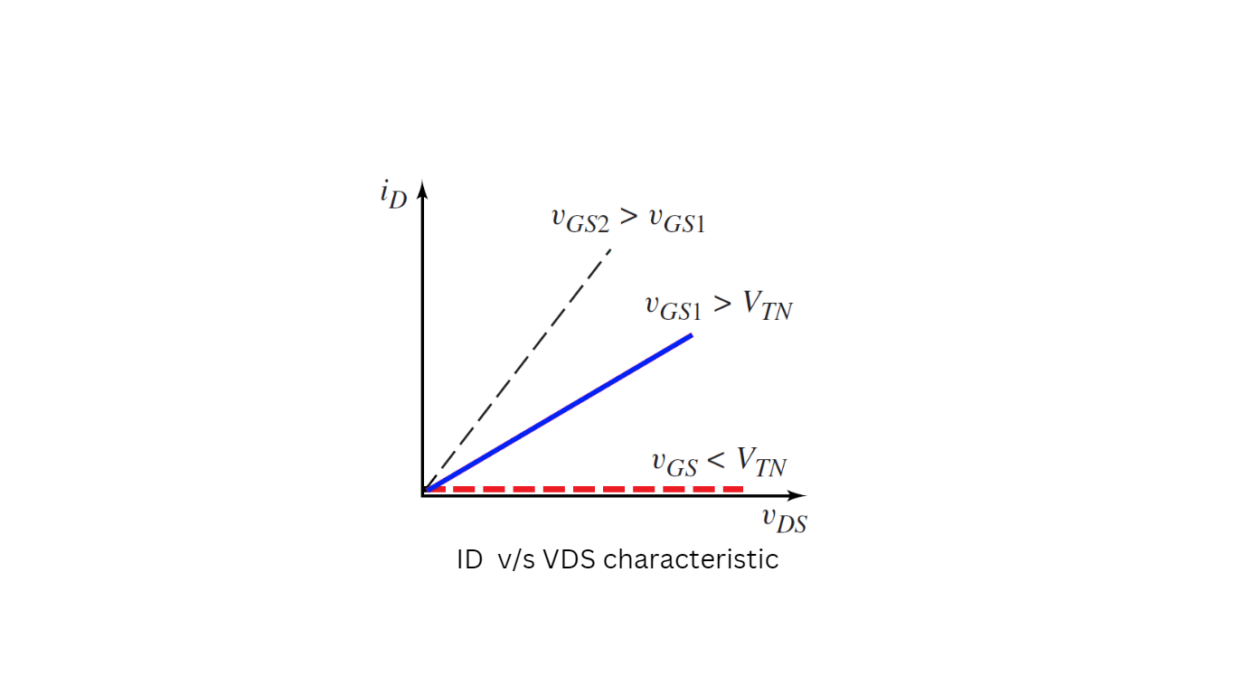
Figure (a), shows the basic MOS structure for the case when VGS > VTN and a small applied VDS. In the figure, the thickness of the inversion channel layer qualitatively indicates the relative charge density, which in this case is essentially constant along the entire channel length. The corresponding ID versus VDS curve is also shown in the figure
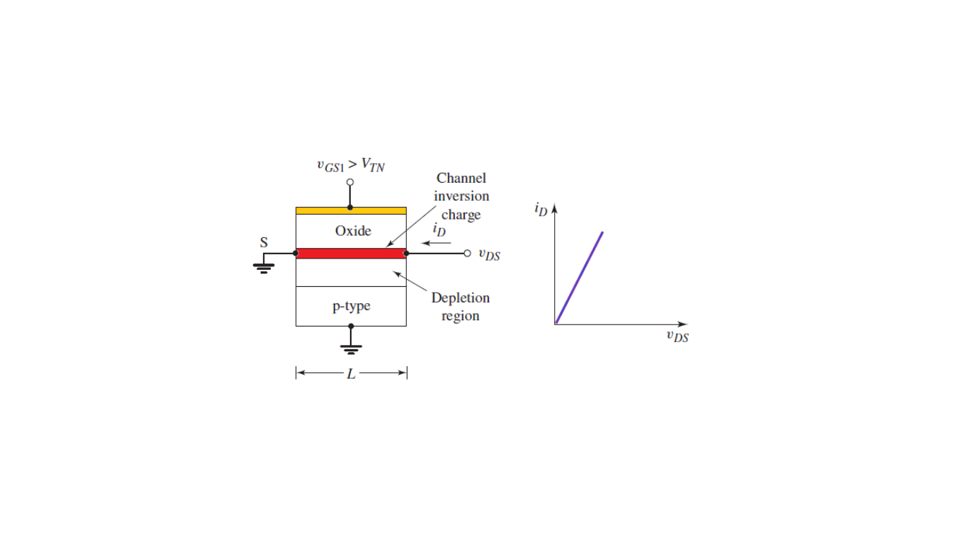
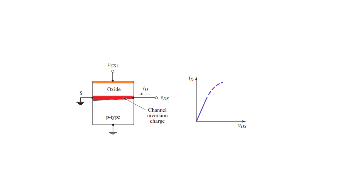
Figure (b), shows the situation when VDS increases. and as the drain voltage increases, the voltage drop across the oxide near the drain terminal decreases, which means that the induced inversion charge density near the drain also decreases. The incremental conductance of the channel at the drain then decreases, which causes the slope of the ID versus VDS curve to decrease. This effect is shown in the ID versus VDS curve in the figure
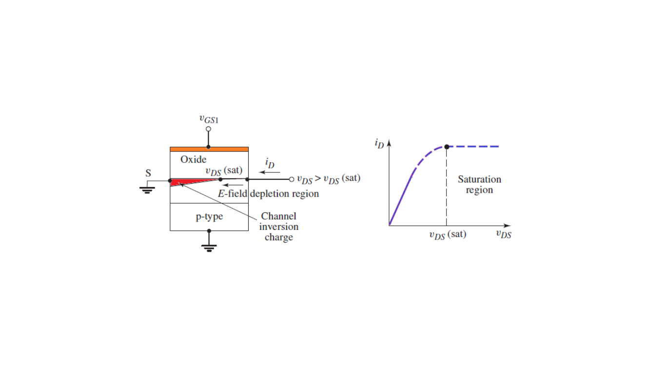
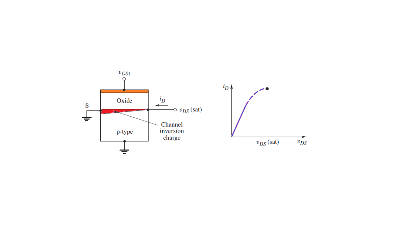
As VDS increases to the point where the potential difference, VGS − VDS, across the oxide at the drain terminal is equal to VTN, the induced inversion charge density at the drain, terminal is zero. This effect is shown schematically in Figure (c). For this condition, the incremental channel conductance at the drain is zero, which means that the slope of the ID versus VDS curve is zero.
When VDS becomes larger than VDS(sat), the point in the channel at which the inversion charge is just zero moves toward the source terminal. In this case, electrons enter the channel at the source, travel through the channel toward the drain, and then, at the point where the charge goes to zero, are injected into the space-charge region, where they are swept by the E-field to the drain contact. In the ideal MOSFET, the drain current is constant for VDS > VDS(sat). This region of the ID versus VDS characteristic is referred to as the saturation region, which is shown in Figure(d).