
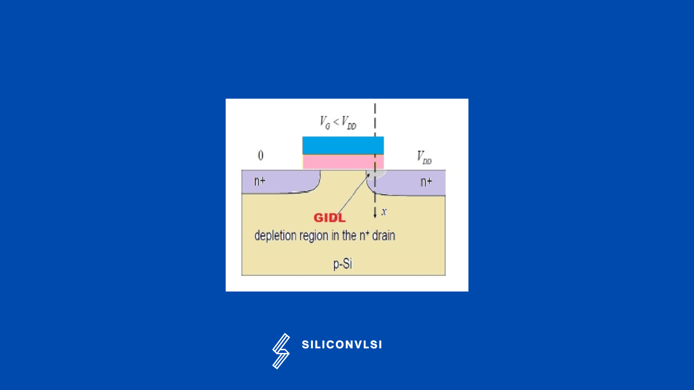
Gate-Induced Drain Leakage – An Overview
GIDL(Gate Induced Drain Leakage) occurs where the gate partially overlaps with the drain of the MOSFET and It is more pronounced when Vds levels are at High potential and Vgs is at low potential. Gate-induced drain leakage current is due to the band-to-band tunneling process in silicon in the gate-to-drain overlap region. This drain leakage current increases with increasing Vd and decreasing Vg.GIDL(Gate Induced Drain Leakage) is directly proportional to the gate-drain overlap area.
Analysis of GIDL(Gate-Induced Drain Leakage) Current:
- For the same Vgs, higher Vds will make the barrier steeper and cause the tunneling easier to happen, so leads to a higher GIDL current. For the same Vds, more negative Vgs will also make the barrier steeper and causes the tunneling easier to happen, so also leads to a higher GIDL current
- Another factor is when a lot of impurities are involved in the drain region, more traps will be formed and it will make the trap-assisted tunneling easier to happen, and hence a higher GIDL current.
How to reduce the GIDL effect:
- Increase the oxide thickness tox to reduce the electric field
- Using Halo Doping
- Using LDD (lightly doped drain: LDD) structure to reduce the electric field near the drain side
- Increase the doping concentration of the drain to decrease the depletion layer width
Conclusion
Gate-induced-drain-leakage (GIDL) current in 45-nm state-of-the-art MOSFETs has been extensively studied. For the current technology node with a 1.2-V power supply voltage, it has been observed that the GIDL current increases in MOSFETs with higher channel-doping levels. Unlike the classical GIDL current generated in the gate-to-drain overlap region, the observed GIDL current is generated by the tunneling of electrons through the reverse-biased channel-to-drain p-n junction. A band-to-band tunneling model has been used to fit the measured GIDL currents under different channel-doping levels and bias conditions, showing good agreement between the modeled results and experimental data. Furthermore, the dependence of the GIDL current on body bias, lateral electric field, channel width, and temperature has been characterized and discussed.