
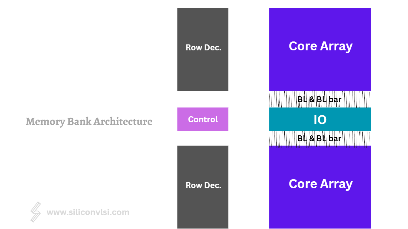
SRAM Memory Bank Architecture
SRAM memory bank architecture is used to reduce the bit line & Bit Bar line load capacitance. SRAM Memory Bank Architecture. We used Common IO in between arrays to reduce the bit line load. SRAM, or static random-access memory, is a type of semiconductor memory that stores data using a flip-flop circuit. Unlike dynamic memory (DRAM), which requires constant refreshing, SRAM can hold data as long as power is supplied. This characteristic enables fast access times and makes SRAM a popular choice for cache memories and high-speed registers.
Importance of Memory Layout Design
The memory layout design of a computer system has a significant impact on its overall performance. It determines how data is organized and accessed, affecting both latency and bandwidth. Efficient memory layout design ensures that data can be accessed quickly, reducing processing delays and improving system responsiveness.
Understanding SRAM Bank Architecture
SRAM bank architecture refers to the organization and arrangement of multiple SRAM banks within a memory subsystem. Each bank consists of a group of SRAM cells and associated control circuitry. The memory controller coordinates the access to these banks, allowing simultaneous read and write operations.
Advantages of SRAM Bank Architecture
Improved Access Time: By dividing the memory into multiple banks, SRAM bank architecture enables parallel access, reducing access time and improving overall system performance.
Increased Bandwidth: With each bank operating independently, SRAM bank architecture allows for concurrent data transfers, increasing the memory’s bandwidth.
Enhanced Fault Tolerance: SRAM banks can be designed with redundancy, allowing for error detection and correction, thus improving the reliability of memory subsystems.
Also Read: Memory Butterfly Architecture
Factors Influencing SRAM Bank Design
Several factors influence the design of SRAM banks, including:
Chip Area: The physical space available on the integrated circuit determines the number of banks that can be implemented.
Access Time: The desired access time for the memory influences the size and organization of each bank.
Power Consumption: The number of banks and associated circuitry affect the overall power consumption of the memory subsystem.
Cost: The cost of implementing multiple banks should be considered in relation to the desired performance benefits.
Also Read:Memory Layout Interview Question
Challenges in SRAM Bank Architecture
Designing an efficient SRAM bank architecture comes with its own set of challenges, including:
Power and Area Overhead: Implementing multiple banks requires additional circuitry, leading to increased power consumption and chip area utilization.
Interference and Coupling: Banks in close proximity can experience interference and coupling effects, leading to performance degradation.
Timing Mismatches: Variations in process, voltage, and temperature can introduce timing mismatches between banks, causing operational issues.