
Steps to Minimize IR Drop in Integrated Circuit Design
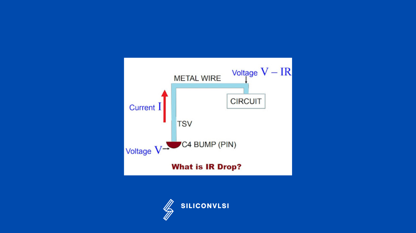
IR drop is the electrical potential difference between two ends of a conducting wire during a current flow. This potential difference depends on this voltage drop across any resistance is the product of current (I) passing through resistance and resistance value (R). (V=IR).
“IR drops relate to Ohm’s Law: Voltage = Current x Resistance”
IR drop, also known as Voltage drop, refers to the difference in voltage between two endpoints of a conducting wire during the flow of current. This drop occurs due to the resistance of the conductor, which determines the percentage of the drop. Essentially, as current flows through the wire, some of the voltage is lost or “dropped” across the wire due to its resistance.
This Voltage drop in the metal wires can weaken the power routing before the actual voltage reaches the power pins of the standard cells in a chip. As a result, it can adversely affect the speed of the standard cells and the overall performance of the chip.
There are two types of IR drops:
- Static
- Dynamic
Static IR Drop:
Static IR drop is an average voltage drop for the design and It is dependent on the RC network of the power grid connecting the power supply to the respective standard cells. The average current depends totally on the time period. Gate-channel leakage current is the major reason for the static IR drop.
Dynamic IR Drop:
Dynamic IR drop is a drop in the voltage due to the high switching activity of transistors(Drain output of the inverter). Dynamic IR drop depends on the switching time of the logic and is less dependent on the clock period. Dynamic IR drop evaluates the IR drop caused when a large number of circuitry switches at the same time, causing peak current demand. It happens when there is an increasing demand for current from the power supply due to switching activities of the chip.
How to reduce the IR Drop-in VLSI?
- Use the proper width of Metal according to current density.
- Use more parallel metal wire strips
- Spread the logic if hotspots are in congested areas.
- Add more proper vias
- Use proper CTS structure.
- Add buffers if the run length of the wire is too long.
- Avoid the jogs in metals
- Using clock gating techniques
If you have both IR drop and congestion, how will you fix it?
In this type of Condition, we should Spread the macros and standard cells, and also we should increase the metal width and the number of straps.
What is the difference between a static IR drop and a dynamic IR drop analysis?
Dynamic IR drop is the drop when the high current draws the power network due to the high switching of the cell(Drain of Inverter). To reduce Dynamic IR drop, reduce the toggle rate or place de-cap cells near high switching cells.