
Multi-Layer Printed Circuit Boards
Boards can be created by stacking multiple layers of substrate cores, resulting in what’s known as multilayer PCBs. An example of such a board is illustrated in Figure 1, comprising three cores and six routing layers (three on the top and three on the bottom). These cores are bonded together using an insulating material that prevents electrical contact between the copper layers of adjacent substrate cores, preventing short circuits.
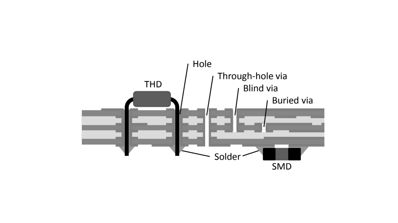
To establish electrical connections between different routing layers, plated-through contacts called vias are used. Vias are formed by drilling holes through the core layers during the initial manufacturing stage. These holes are then coated with copper to make them conductive. Depending on their location, these vias are categorized as buried, blind, or through-hole vias.
There are two primary methods for mounting components on PCBs:
Through-Hole Technology (THT)
Devices with leads are inserted into holes, typically through-hole vias, and soldered in position.
Surface-Mount Technology (SMT)
Components possess metal pads for connection to the surface of the board.
Associated with these methods are through-hole devices (THDs) for THT and surface-mount(ed) devices (SMDs) for SMT.
Solder is used to connect components in THT, whereas in SMT, metal pads on components are soldered to the surface of the board. Copper layers in the PCB facilitate interconnections, and substrate cores are separated by bonding agents known as “prepreg.”
Integrated circuits (ICs)
Integrated circuits (ICs), apart from discrete components, can also be mounted on PCBs. However, ICs need to be enclosed in the packaging. Sometimes, unpackaged ICs (bare dies) are directly mounted on PCBs, but the stability of the connection is crucial due to the varying thermal expansion rates of semiconductors and boards. The mounting technologies, THT and SMT, can also be combined. Surface-mount technology (SMT) is more widely used due to its advantages, including ease of handling, high packing densities, and the ability to mount components on both sides of the PCB.