

NAND Gate: Working, CMOS Advantages & Layout Explained
A NAND gate is one of the most important logic gates used in digital electronics and CMOS VLSI design. It produces a LOW output only when all of its inputs are HIGH. For every other input combination, the output remains HIGH.
In CMOS technology, a NAND gate is implemented using complementary PMOS and NMOS transistor networks. Understanding both its logical operation and physical layout is important for learning standard-cell design and VLSI layout.
What Is a NAND Gate?
A NAND gate is an AND gate followed by an inverter.
For a two-input NAND gate:
Y = (A · B)’
where:
- A and B are the inputs.
- Y is the output.
'represents logical inversion.
The output is LOW only when both A and B are HIGH.
NAND Gate Truth Table
| A | B | Y = (A·B)’ |
|---|---|---|
| 0 | 0 | 1 |
| 0 | 1 | 1 |
| 1 | 0 | 1 |
| 1 | 1 | 0 |
This simple truth table explains the operation of the CMOS transistor network.
CMOS NAND Gate Circuit
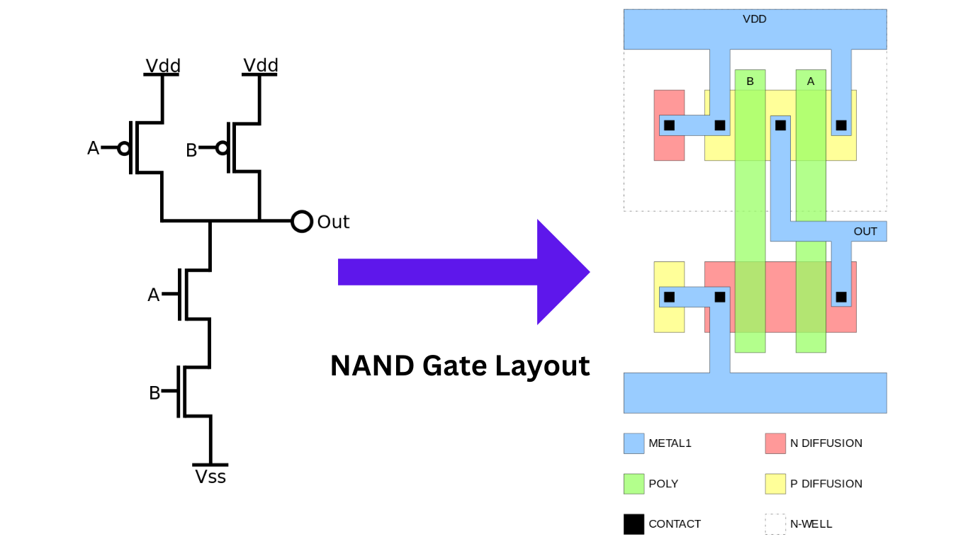
A conventional two-input CMOS NAND gate uses:
- 2 PMOS transistors in parallel
- 2 NMOS transistors in series
The PMOS network forms the pull-up network (PUN), while the NMOS network forms the pull-down network (PDN).


How Does a CMOS NAND Gate Work?
The operation can be understood by examining the PMOS and NMOS networks for each input combination.
Case 1: A = 0 and B = 0
Both inputs are LOW.
Therefore:
- Both NMOS transistors are OFF.
- Both PMOS transistors are ON.
- A conductive path exists from VDD to the output.
Therefore:
Output = 1
Case 2: A = 0 and B = 1
For A = 0:
- PMOS controlled by A → ON
- NMOS controlled by A → OFF
For B = 1:
- PMOS controlled by B → OFF
- NMOS controlled by B → ON
Because the two NMOS transistors are connected in series, the OFF NMOS transistor breaks the path to ground.
At the same time, the ON PMOS provides a path from VDD to the output.
Therefore:
Output = 1
Case 3: A = 1 and B = 0
This is the complementary case.
- One PMOS is ON.
- One PMOS is OFF.
- One NMOS is ON.
- One NMOS is OFF.
The series NMOS path to ground is broken.
Therefore:
Output = 1
Case 4: A = 1 and B = 1
Both inputs are HIGH.
Therefore:
- Both NMOS transistors are ON.
- Both PMOS transistors are OFF.
- The series NMOS network creates a conductive path from output to VSS.
Therefore:
Output = 0
This is the only condition that produces a LOW output.
Why Are PMOS Transistors in Parallel?
A NAND gate must produce HIGH whenever at least one input is LOW.
A PMOS transistor turns ON when its gate input is LOW.
Therefore, connecting the PMOS devices in parallel ensures that if either A or B is LOW, there is a pull-up path from VDD to the output.
In Boolean terms:
Pull-up condition = A’ + B’
Using De Morgan’s law:
A’ + B’ = (A · B)’
which is exactly the NAND function.
Why Are NMOS Transistors in Series?
A NAND gate should pull the output LOW only when both inputs are HIGH.
An NMOS transistor turns ON when its gate input is HIGH.
Therefore, the NMOS devices are connected in series.
Both must be ON before a complete path from the output to VSS exists.
Thus:
Pull-down condition = A · B
This produces the required NAND operation.
CMOS Advantage
CMOS logic has several important advantages compared with older NMOS logic families.
Fast Pull-Up and Pull-Down
In CMOS, both the pull-up and pull-down networks use transistors rather than relying on a passive resistor for one of the transitions.
When the appropriate network is active, it provides a relatively low-resistance path to the supply rail.
Therefore, CMOS can provide efficient:
- Low-to-high transitions
- High-to-low transitions
The actual propagation delay depends on transistor sizing, load capacitance, supply voltage, process technology, and circuit topology.
Full Logic Swing
A properly designed static CMOS gate can produce an output close to:
Logic HIGH → VDD
Logic LOW → VSS
This provides good noise margins and allows CMOS gates to be cascaded effectively.
Low Static Power
When a static CMOS gate is in a stable logic state, ideally there is no direct DC path from VDD to VSS.
Therefore, ideal static CMOS has very low static power consumption.
In real circuits, leakage currents still exist, particularly in modern scaled technologies.
Good Noise Immunity
The near-rail-to-rail output swing provides good logic-level separation and contributes to the strong noise margins associated with CMOS logic.
CMOS NAND Gate Delay
The propagation delay of a CMOS NAND gate depends on factors such as:
- Transistor resistance
- Load capacitance
- Input transition time
- Supply voltage
- Transistor sizing
- Number of series transistors
The logical effort method can be used to compare and estimate the delay of CMOS logic gates.
For a NAND gate, the series NMOS network is particularly important because series devices increase the effective pull-down resistance.
NAND Gate Layout
The schematic of a NAND gate describes the electrical connectivity, while the layout represents how the transistors and interconnects are physically implemented on silicon.
The layout is created using process-specific layers such as:
- N-well
- Active/diffusion
- Polysilicon
- Contacts
- Metal
- Additional metal and via layers
The exact layer names, colors, and design rules depend on the semiconductor process and PDK.

How Transistors Are Formed in the Layout
In a conventional CMOS process:
- NMOS devices are formed in the appropriate p-type body region.
- PMOS devices are formed inside an n-well in a conventional n-well CMOS process.
- Polysilicon crossing an active region forms the transistor gate.
- Contacts connect device regions to metal.
- Metal layers provide signal and power interconnections.
Therefore, the transistor does not exist simply because a single layer is drawn. It is created by the interaction of multiple process layers.
NAND Gate Physical Structure
A typical two-input NAND layout contains:
PMOS Network
The two PMOS devices are arranged in parallel.
Their sources are connected toward VDD, while their drain regions contribute to the output network.
NMOS Network
The two NMOS devices are arranged in series.
The series connection creates the required pull-down path when both inputs are HIGH.
Polysilicon Inputs
The input signals A and B can be routed using polysilicon gates crossing the active regions.
Where polysilicon crosses active diffusion, a MOS transistor is formed.
Metal Output
The output node connects the appropriate PMOS and NMOS drain regions.
Metal is commonly used to route the output to other cells or circuit blocks.
Contacts in NAND Layout
Contacts provide electrical connections between transistor-related layers and the appropriate metal layer.
For example, a contact can connect:
- Diffusion to Metal
- Polysilicon to Metal
The exact contact naming and layer stack depends on the process technology.
VDD and VSS Connections
The NAND cell requires connections to the two supply rails:
- VDD → positive supply
- VSS → ground/reference supply
The PMOS network is connected toward VDD, while the NMOS network is connected toward VSS.
This allows the gate to switch the output between the two supply rails.
Well and Substrate Taps
Proper body connections are essential in CMOS layout.
In a conventional n-well CMOS process:
- A p-type substrate/body tap is connected to VSS.
- An n-well tap is connected to VDD.
These connections keep the body regions at the intended potentials and help reduce the risk of latch-up.
The exact implementation depends on the process and standard-cell layout rules.
NAND Gate Layout vs. NAND Gate Schematic
| Feature | NAND Schematic | NAND Layout |
|---|---|---|
| Represents | Electrical behavior/connectivity | Physical implementation |
| Main elements | PMOS and NMOS symbols | Process layers |
| Inputs | A, B | Poly/metal routing |
| Output | Logic node | Physical interconnect |
| Transistor formation | Symbolically defined | Created by layer interaction |
| VDD/VSS | Circuit connections | Physical power rails |
| Verification | Logic/connectivity | DRC, LVS and related checks |
From NAND Schematic to Silicon Layout
A simplified design flow is:
Logic function
↓
CMOS transistor schematic
↓
Transistor sizing
↓
Physical layout
↓
Design Rule Check (DRC)
↓
Layout Versus Schematic (LVS)
↓
Parasitic extraction
↓
Post-layout simulation
This process ensures that the physical implementation correctly represents the intended circuit and satisfies manufacturing rules.
Why Is NAND Gate Important in VLSI?
NAND is a universal logic gate.
This means that other basic logic functions can be constructed using NAND gates.
For example:
NOT Using NAND
Connect both inputs together:
Y = (A · A)’ = A’
Therefore, a NAND gate can function as an inverter.
AND Using NAND
First NAND the inputs and then invert the result:
Y = ((A · B)’)’ = A · B
OR Using NAND
Using De Morgan’s law:
A + B = (A’ · B’)’
The inverted inputs can themselves be generated using NAND gates.
This makes NAND gates extremely important in digital logic and CMOS VLSI design.
NAND Gate vs. NOR Gate
Both NAND and NOR are universal gates, but their CMOS transistor arrangements are complementary.
| Feature | NAND | NOR |
|---|---|---|
| PMOS network | Parallel | Series |
| NMOS network | Series | Parallel |
| Pull-down condition | All inputs HIGH | Any input HIGH |
| Pull-up condition | Any input LOW | All inputs LOW |
| Universal gate | Yes | Yes |
For a two-input gate, the NAND pull-down path contains two series NMOS devices, while the NOR pull-up path contains two series PMOS devices. Since PMOS devices generally have lower mobility than NMOS devices, transistor sizing and delay characteristics differ between NAND and NOR gates.
Common Questions About NAND Gates
What is a NAND gate?
A NAND gate is a logic gate whose output is the complement of the AND operation:
Y = (A · B)’
The output becomes LOW only when all inputs are HIGH.
How many transistors are required for a CMOS NAND gate?
A conventional 2-input static CMOS NAND gate requires four transistors:
- 2 PMOS
- 2 NMOS
For an N-input static CMOS NAND gate, the basic transistor count is generally 2N.
Why are NMOS transistors connected in series in a NAND gate?
The output should become LOW only when all inputs are HIGH. Series NMOS devices ensure that a complete pull-down path exists only when every NMOS transistor is ON.
Why are PMOS transistors connected in parallel?
A NAND output should become HIGH when any input is LOW. Parallel PMOS devices provide a pull-up path whenever at least one PMOS is turned ON.
What happens when both NAND inputs are HIGH?
Both NMOS transistors turn ON and both PMOS transistors turn OFF.
The output is therefore connected to VSS through the series NMOS network:
A = 1, B = 1 → Y = 0
What happens when one NAND input is LOW?
The corresponding PMOS transistor turns ON and the corresponding NMOS transistor turns OFF.
The series NMOS path is broken, while the PMOS network provides a path to VDD.
Therefore:
Y = 1
Why is NAND called a universal gate?
NAND can be used to construct NOT, AND, OR, and other logic functions. Therefore, complete digital logic systems can be implemented using NAND gates.
Key Takeaways
- A NAND gate implements Y = (A · B)’.
- A conventional 2-input CMOS NAND uses 2 PMOS + 2 NMOS transistors.
- PMOS transistors are connected in parallel.
- NMOS transistors are connected in series.
- The output becomes LOW only when all inputs are HIGH.
- CMOS provides near-rail-to-rail logic levels and good noise margins.
- A NAND layout represents the physical implementation using process-specific layers.
- Polysilicon crossing active material forms MOS transistor gates.
- Contacts and metal layers provide electrical interconnections.
- Well and substrate taps establish proper body potentials and help prevent latch-up.
- NAND is a universal logic gate and is widely used in CMOS VLSI.