
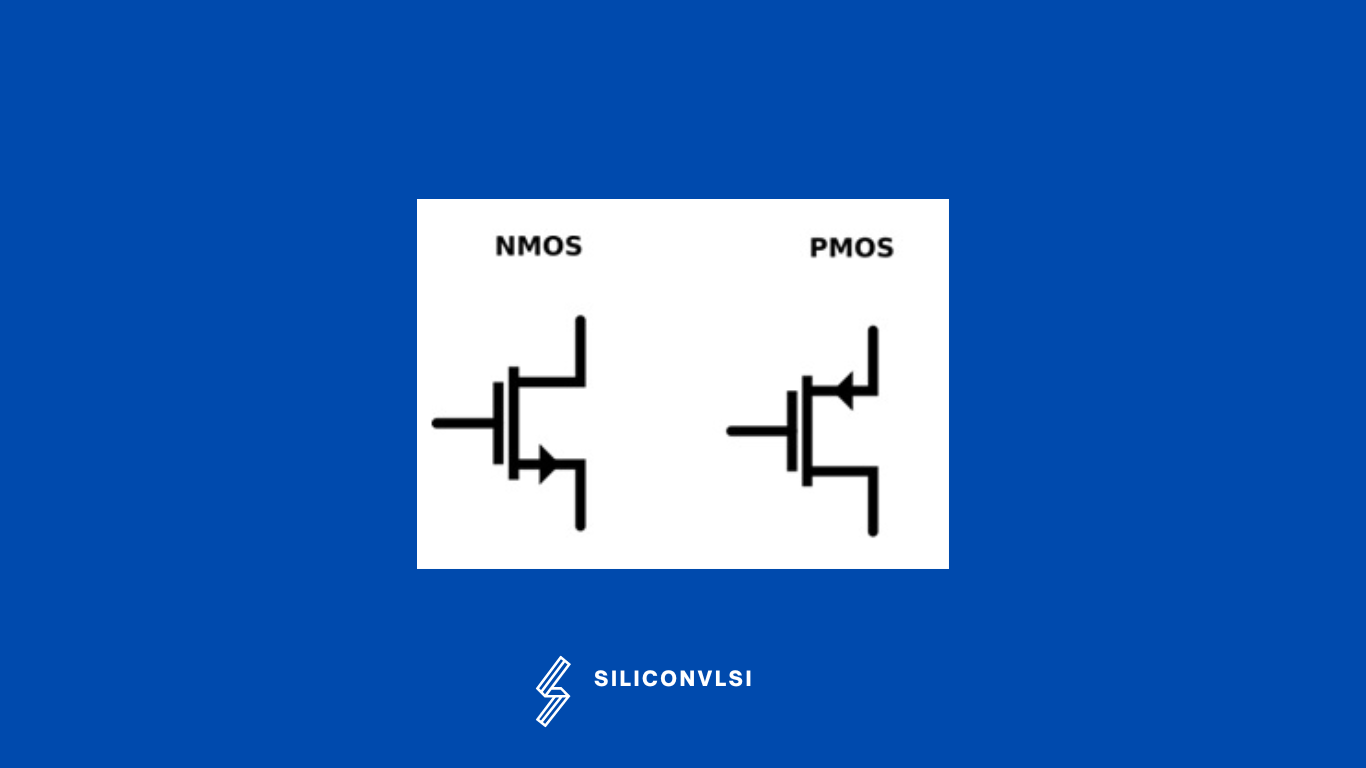
NMOS and PMOS Models
There are two types of MOSFETs: NMOS and PMOS. NMOS uses N-type doped semiconductors as the source and drains and P-type as the substrate, whereas PMOS is the opposite. The polarity of the voltage: the threshold voltage VTH, the VGS, and the VDS are negative. Secondly, the charge carriers are not the same: NMOS uses electrons and PMOS uses holes as majority carriers.
NMOS advantage.
- NMOS is faster than PMOS.
- The ON resistance of an NMOS is almost half of a PMOS.
- NMOS transistors provide a smaller footprint than PMOS for the same output current.
NMOS and PMOS ModelsMOS transistors are built on top of silicon wafers. This process uses semiconductor doping and oxide growth to create N-type, P-type, and insulating regions.
The drain and source regions are strongly doped with N-dopants (NMOS) or P-dopants (PMOS), and the substrate is doped with the opposite type (P-type for NMOS and N-type for PMOS). The gate is connected to a thin layer of silicon dioxide, that insulates the gate connection from the substrate. When enough charge is accumulated in that region, the minority carriers become the majority carriers, forming a channel with the same type as the drain and source. This is why NMOS requires positive voltages (to attract electrons) and PMOS requires negative voltages (to attract holes) for channel formation.
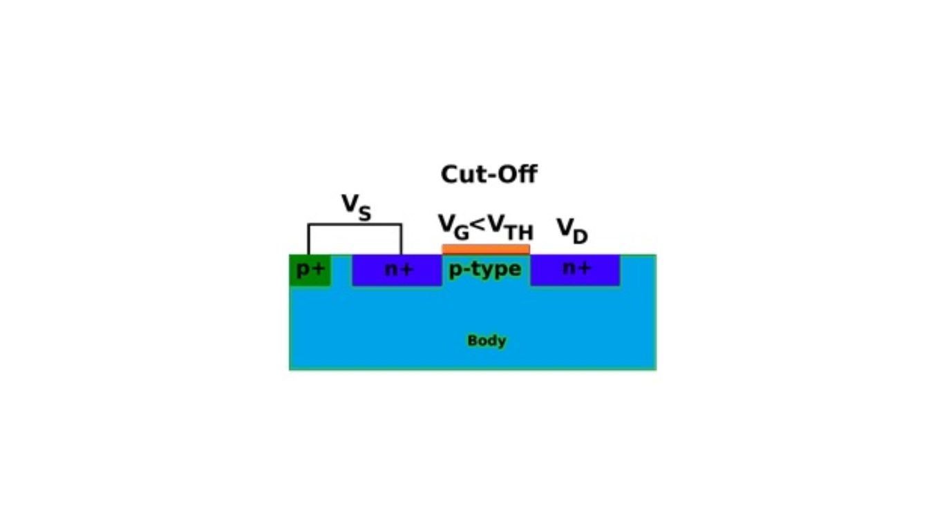
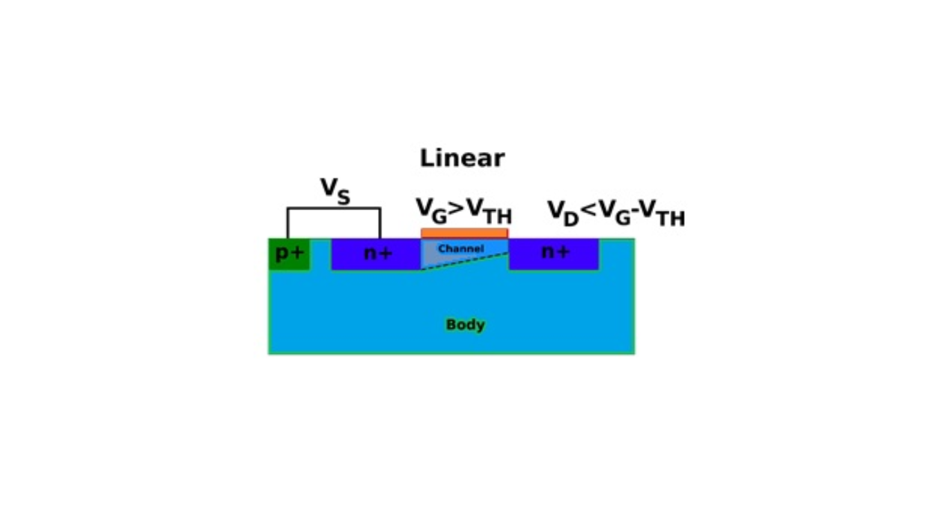
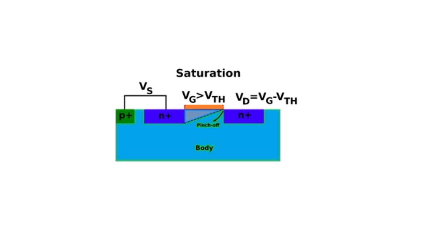
In electronic terms, the working principle of a transistor is very simple, it has three main terminals, Gate, Drain & Source. In the case of a MOSFET, The relationship between the drain current (ID) and the gate-to-source voltage (VGS) is highly non-linear, and it is divided into three operating regions. Each region has its own conditions, properties, and equations, as described in the following Table

Region of Operation of CMOS Inverter
In the cut-off region, the transistor acts as an open circuit between drain and source, in the linear region the relation between VDS and ID is almost ohmic, and in the saturation mode, the current is – ideally – independent on VDS.
Cut Off region
In this region, the transistor will be off or its act as an open circuit.
Linear region
In Linearregion the relation between VDS and ID is almost ohmic. so we can say that it’s an ohmic region. which is very useful in amplifiers.
Saturation region
Saturation mode is independent of Vds. In the saturation or linear region, the transistor will be biased so that the maximum amount of gate voltage is applied to the device which results in the channel resistance RDS.
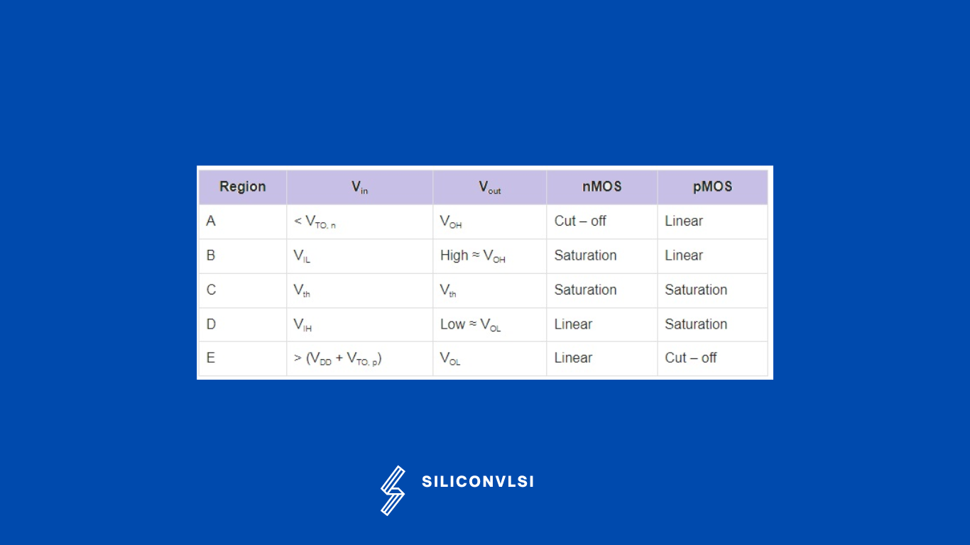
For the different values of input voltages, the operating regions are listed below for both transistors
The channel presents ohmic resistance for a fixed VGS (linear operation mode) as long as VDS remains smaller than the VGS – VTH. After that, the charge concentration near the drain is nulled, and the channel becomes “pinched”. This is called channel pinch-off and marks the division between the saturation and linear regions. As VDS increases, the pinch point moves and the effective length of the channel reduces, which results in the channel-length modulation effect discussed previously.
Why do we use NMOS instead of PMOS for designing the logic gates?
For the same output current, NMOS transistors have a smaller footprint compared to PMOS transistors, and they also operate faster. In CMOS technology, NMOS transistors are typically used in the pull-down network, while PMOS transistors are used in the pull-up network. CMOS is preferred over NMOS for embedded system design.