Close Menu
  • Analog Design
    • Latest Analog Layout Interview Questions (2025)
  • Digital Design
    • Digital Electronics Interview Question(2025)
    • Top VLSI Interview Questions
  • Physical Design
    • Physical Design Interview Questions for VLSI Engineers
  • Verilog
    • Verilog Interview Questions(2024)
  • Forum
Facebook Instagram YouTube LinkedIn WhatsApp
SiliconvlsiSiliconvlsi
Forum Questions Register in Forum Login in Forum
Facebook Instagram YouTube LinkedIn WhatsApp
  • Analog Design
    • Latest Analog Layout Interview Questions (2025)
  • Digital Design
    • Digital Electronics Interview Question(2025)
    • Top VLSI Interview Questions
  • Physical Design
    • Physical Design Interview Questions for VLSI Engineers
  • Verilog
    • Verilog Interview Questions(2024)
  • Forum
SiliconvlsiSiliconvlsi
Home»VLSI Design»Steps in VLSI Physical Design Flow
VLSI Design

Steps in VLSI Physical Design Flow

siliconvlsiBy siliconvlsiSeptember 20, 2021Updated:May 28, 2024No Comments1 Min Read
Facebook Pinterest LinkedIn Email WhatsApp
Share
Facebook Twitter LinkedIn Pinterest Email

 Steps in VLSI Physical Design Flow

The system’s actual input and output processes are related to the physical design. This is described in terms of the integration of data into a system, its processing, verification, and authentication, as well as its display. The following system requirements are chosen during physical design.
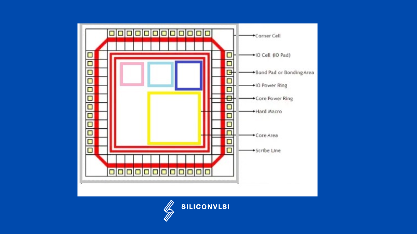
Floorplanning

Floorplanning helps to determine the locations, shape, and size of modules in a chip, and as such it estimates the chip area, delay, and wiring congestion, thereby providing a groundwork for layout.
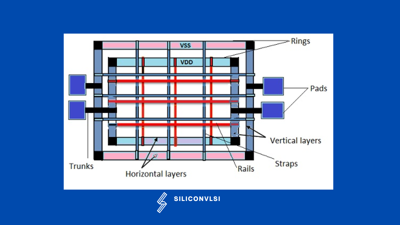

Read More

Power Panning

One of the most important stages in physical design is power planning. It will be utilized to supply power to macros and standard cells while staying under the IR-Drop limit.


Share. Facebook Twitter Pinterest LinkedIn Tumblr Email

Related Posts

How Shielding Avoids Crosstalk Problem? What Exactly Happens There?

September 22, 2024

Navigating the Challenges of Gate Dielectric Scaling in MOS Transistors

August 1, 2024

Challenges in Modern SoC Design Verification

April 20, 2024
Leave A Reply Cancel Reply

Facebook X (Twitter) Instagram Pinterest Vimeo YouTube
  • About Us
  • Contact Us
  • Privacy Policy
© 2025 Siliconvlsi.

Type above and press Enter to search. Press Esc to cancel.