
What is Ripple Carry Adder?
To understand Ripple Carry Adder, we need to be familiar with two basic building blocks: the half adder and the full adder.
Half Adder
A half adder is a simple circuit that adds two bits and produces the sum and carries outputs. It doesn’t consider any incoming carry from previous stages. The truth table for a half-adder is as follows:
| A | B | Sum | Carry |
|---|---|---|---|
| 0 | 0 | 0 | 0 |
| 0 | 1 | 1 | 0 |
| 1 | 0 | 1 | 0 |
| 1 | 1 | 0 | 1 |
Full Adder
A full adder is an extension of the half adder that takes into account the incoming carry from previous stages. It adds three bits: two inputs (A and B) and a carry-in (Cin), and produces the sum and carries outputs. The truth table for a full adder is as follows:
| A | B | Cin | Sum | Carry |
|---|---|---|---|---|
| 0 | 0 | 0 | 0 | 0 |
| 0 | 0 | 1 | 1 | 0 |
| 0 | 1 | 0 | 1 | 0 |
| 0 | 1 | 1 | 0 | 1 |
| 1 | 0 | 0 | 1 | 0 |
| 1 | 0 | 1 | 0 | 1 |
| 1 | 1 | 0 | 0 | 1 |
| 1 | 1 | 1 | 1 | 1 |
Ripple Carry Adder Architecture
The Ripple Carry Adder is formed by cascading full adders together, with the carry output of each stage connected to the carry input of the next stage. The block diagram of a 4-bit Ripple Carry Adder is shown below:
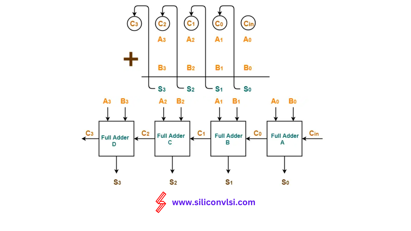
The operation of a Ripple Carry Adder is straightforward. Each full adder receives two bits from the input operands and the carry-in from the previous stage. The sum output of each full adder becomes one bit of the final sum, and the carry output propagates to the next stage as the carry-in.
Advantages of Ripple Carry Adder
Simplicity: Ripple Carry Adder is relatively simple to design and implement.
Low hardware requirements: It requires minimal hardware resources compared to other adder architectures.
Ease of scalability: The Ripple Carry Adder can be easily expanded to handle larger bit widths by cascading additional full adders.
Applications of Ripple Carry Adder
Ripple Carry Adders find applications in various digital systems, including:
- Arithmetic logic units (ALUs)
- Microprocessors
- Digital signal processing (DSP) units
- Data processing units
Working Of 4-bit Ripple Carry Adder-
- The two 4-bit numbers are 0101 (A3A2A1A0) and 1010 (B3B2B1B0).
- These numbers are to be added using a 4-bit ripple carry adder.
4-bit Ripple Carry Adder carries out the addition as explained in the following stages-
Stage-01
- When Cin is fed as input to the full Adder A, it activates the full adder A.
- Then at full adder A, A0 = 1, B0 = 0, Cin = 0.
Full adder A computes the sum bit and carry bit as-
Calculation of S0
S0 = A0 ⊕ B0 ⊕ Cin
S0 = 1 ⊕ 0 ⊕ 0
S0 = 1
Calculation of C0
C0 = A0B0 ⊕ B0Cin ⊕ CinA0
C0 = 1.0 ⊕ 0.0 ⊕ 0.1
C0 = 0 ⊕ 0 ⊕ 0
C0 = 0
Stage-02
- When C0 is fed as input to the full adder B, it activates the full adder B.
- Then at full adder B, A1 = 0, B1 = 1, C0 = 0.
Full adder B computes the sum bit and carry bit as-
Calculation of S1
S1 = A1 ⊕ B1 ⊕ C0
S1 = 0 ⊕ 1 ⊕ 0
S1 = 1
Calculation of C1
C1 = A1B1 ⊕ B1C0 ⊕ C0A1
C1 = 0.1 ⊕ 1.0 ⊕ 0.0
C1 = 0 ⊕ 0 ⊕ 0
C1 = 0
Stage-03
- When C1 is fed as input to the full adder C, it activates the full adder C.
- Then at full adder C, A2 = 1, B2 = 0, C1 = 0.
Full adder C computes the sum bit and carry bit as-
Calculation of S2
S2 = A2 ⊕ B2 ⊕ C1
S2 = 1 ⊕ 0 ⊕ 0
S2 = 1
Calculation of C2
C2 = A2B2 ⊕ B2C1 ⊕ C1A2
C2 = 1.0 ⊕ 0.0 ⊕ 0.1
C2 = 0 ⊕ 0 ⊕ 0
C2 = 0
Stage-04
- When C2 is fed as input to the full adder D, it activates the full adder D.
- Then at full adder D, A3 = 0, B3 = 1, C2 = 0.
Full adder D computes the sum bit and carry bit as-
Calculation of S3
S3 = A3 ⊕ B3 ⊕ C2
S3 = 0 ⊕ 1 ⊕ 0
S3 = 1
Calculation of C3
C3 = A3B3 ⊕ B3C2 ⊕ C2A3
C3 = 0.1 ⊕ 1.0 ⊕ 0.0
C3 = 0 ⊕ 0 ⊕ 0
C3 = 0
Thus finally,
- Output Sum = S3S2S1S0 = 1111
- Output Carry = C3 = 0