
Subthreshold Leakage
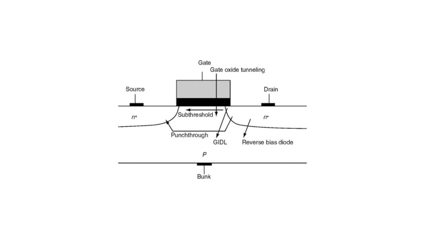
or in other words when the gate-to-source voltage is below the threshold voltage of the device. This leakage current is caused by a few electrons that have enough thermal energy to surmount the energy barrier caused by the built-in potential, creating a weak inversion layer and allowing a small degree of conduction to occur.
This phenomenon can occur in both PMOS and NMOS transistors. As semiconductor devices continue to scale down in size according to Moore’s law, the subthreshold leakage current is becoming a major portion of total power dissipation in CMOS digital circuits, leading to higher energy consumption and decreased battery life in portable devices.
Minimizing subthreshold leakage is a key goal in the design of low-power integrated circuits, and it typically involves the careful management of threshold voltages and device sizing, as well as the use of more advanced techniques such as power gating, multi-threshold CMOS (MTCMOS) design, and adaptive body biasing.