Close Menu
  • Analog Design
    • Latest Analog Layout Interview Questions (2025)
  • Digital Design
    • Digital Electronics Interview Question(2025)
    • Top VLSI Interview Questions
  • Physical Design
    • Physical Design Interview Questions for VLSI Engineers
  • Verilog
    • Verilog Interview Questions(2024)
  • Forum
Facebook Instagram YouTube LinkedIn WhatsApp
SiliconvlsiSiliconvlsi
Forum Questions Register in Forum Login in Forum
Facebook Instagram YouTube LinkedIn WhatsApp
  • Analog Design
    • Latest Analog Layout Interview Questions (2025)
  • Digital Design
    • Digital Electronics Interview Question(2025)
    • Top VLSI Interview Questions
  • Physical Design
    • Physical Design Interview Questions for VLSI Engineers
  • Verilog
    • Verilog Interview Questions(2024)
  • Forum
SiliconvlsiSiliconvlsi
Home»VLSI Design»What is accumulation region in MOSFET?
VLSI Design

What is accumulation region in MOSFET?

siliconvlsiBy siliconvlsiJanuary 8, 2022Updated:April 29, 2024No Comments1 Min Read
Facebook Pinterest LinkedIn Email WhatsApp
Share
Facebook Twitter LinkedIn Pinterest Email

Accumulation region in MOSFET

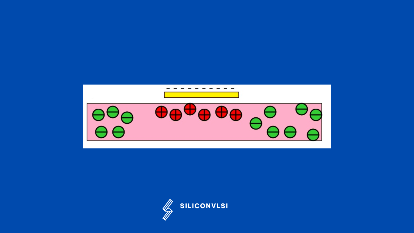
MOSFET means Metal oxide semiconductor Field-effect Transistor.For this explanation Consider NMOS Transitore to understand accumulation, This means it has a p-type substrate, which means the substrate has holes as the majority of carriers throughout the substrate.

Now apply a negative voltage to the Gate, this voltage causes holes in the substrate to come near to the interface. Before applying voltage there were already holes present in the p substrate and after applying the negative voltage few more holes are moved toward the interface, in simple words same carriers are accumulating. This is called Accumulation.

Why a MOSFET in accumulation mode is not conducting?

When a negative voltage is applied to the gate, holes are attracted to the semiconductor-insulator interface, creating a conducting surface that extends from the bulk to the interface. However, because both the source and drain are n-type, in accumulation mode, the transistor behaves like an npn transistor, where the source and drain are insulated by two reverse-biased pn junctions. As a result, electrons in the source cannot flow to the drain, and no conduction channel is formed.


Share. Facebook Twitter Pinterest LinkedIn Tumblr Email

Related Posts

How Shielding Avoids Crosstalk Problem? What Exactly Happens There?

September 22, 2024

Navigating the Challenges of Gate Dielectric Scaling in MOS Transistors

August 1, 2024

Challenges in Modern SoC Design Verification

April 20, 2024
Leave A Reply Cancel Reply

Facebook X (Twitter) Instagram Pinterest Vimeo YouTube
  • About Us
  • Contact Us
  • Privacy Policy
© 2025 Siliconvlsi.

Type above and press Enter to search. Press Esc to cancel.