
Insertion Delay Meaning and Examples
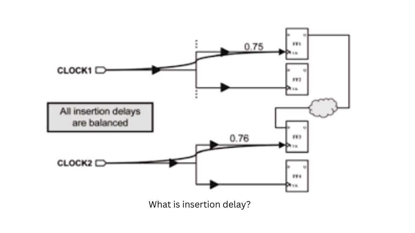
In the context of integrated circuit (IC) design, insertion delay refers to the additional delay introduced by inserting a component or circuit element into a signal path. It represents the increase in propagation time that occurs when a device or circuit is added to the original path.
When a signal travels through a circuit, it encounters various components, such as logic gates, buffers, or interconnects. Each of these components introduces a certain amount of delay due to the finite time it takes for the signal to propagate through them. This delay can be influenced by factors such as the physical distance, the electrical characteristics of the components, and the load capacitance they drive.
Insertion delay occurs when a new component is added to an existing signal path. This component can be a new logic gate, a memory element, or any other circuit element. When the new component is connected to the signal path, it introduces an additional propagation delay, altering the overall timing behavior of the circuit.
The magnitude of the insertion delay depends on various factors, including the characteristics of the added component, the interconnect lengths, and the fan-out or fan-in of the signals. Additionally, factors such as process technology, supply voltage, and temperature can also impact the insertion delay.
Designers need to consider insertion delay when designing circuits, especially in high-speed applications or when meeting strict timing requirements is important. By accurately estimating and accounting for insertion delays, designers can ensure proper timing synchronization, avoid signal integrity issues, and optimize the overall performance of the circuit.
It’s important to note that insertion delay is different from the intrinsic delay of a component, which refers to the inherent delay associated with the operation of a single device. Insertion delay specifically refers to the delay introduced by adding the component into an existing signal path, taking into account the interaction with the surrounding circuitry and interconnects.