
Pinch off effect
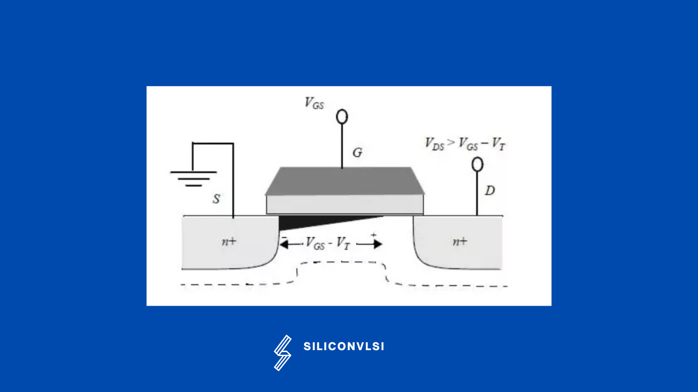
When we increase the drain voltage substantially(Vds> Vgs-Vt, called the saturation voltage), The drain voltage becomes large enough that the gate-to-substrate potential at the drain is smaller than the threshold. Therefore, the channel thickness at this end goes to zero, which we call a “pinch-off” condition in MOSFET.
What is a MOSFET transistor?
The MOSFET (Metal Oxide Silicon Field Effect Transistor) is a device that controls a current between two contacts (Source and Drain) using a voltage contact (Gate). The device uses a surface effect to create an n-type region in a p-type substrate.
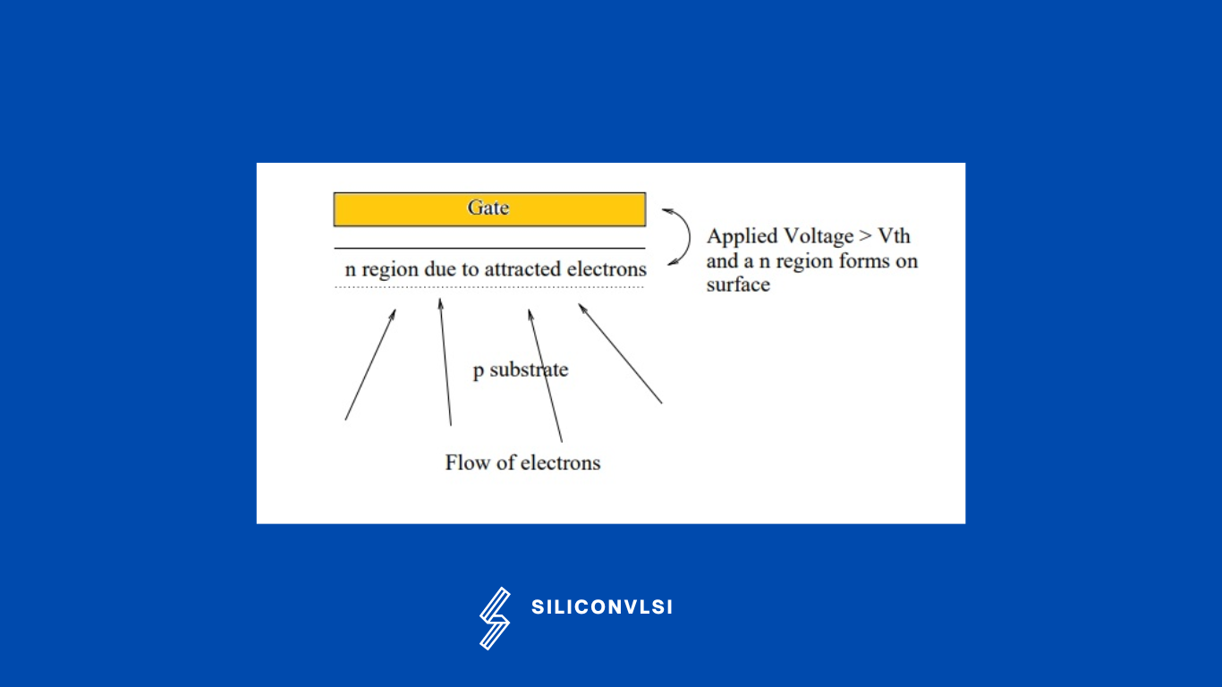
To understand this we take a simple capacitor structure using a p-type substrate oxide layer and a metal gate. If we apply a positive potential to the gate, electrons will be attracted to the gate and will pile up at the surface underneath the gate. At some voltage, Vt called the threshold voltage the region under the gate will have enough additional electrons that n>p and the material will be n-type, not p-type. The oxide is very important as it stops the current flow toward the gate. It will also force the electrons to collect underneath the gate and turn the material n-type.
What is Channel in Mosfet?
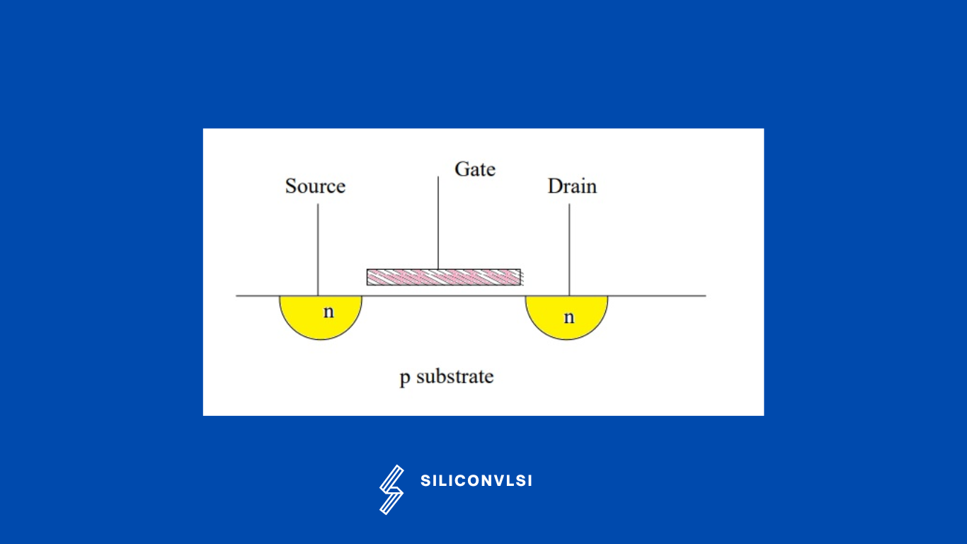
The basic MOSFET structure uses the capacitor structure above with n-type regions placed, known as the source and drain. The basic operation of the device is to bias the gate with Vg>vt and form an n-type region between the source and the drain. This provides a simple n-type path between the n-type source and drains regions for electrons to flow. This region is called a channel.
A channel is created between the source and drain when the gate is given the proper voltage. So that charges can go from the source to the drain, we have essentially built a pipe between them. The voltage is then applied between the source and drain. A charge will begin to transfer between the source and drain as a result. But it will also alter the channel’s shape
The formation of this channel provides a simple resistive path between the source and the drain. The thickness of the channel is a function of the difference between the gate potential and the potential in the substrate(source).
Now, when we applied gate voltage and Vds>Vgds-Vt, the saturation region will start. For larger drain biases, the drain current saturates and becomes independent of the drain bias, which is called a saturation region.
What happens if Vds> Vgs – Vt?, Depletion region separating the pinch-off and drain widens, In the Pinch-off condition, the Id will be constant due to the depletion region.
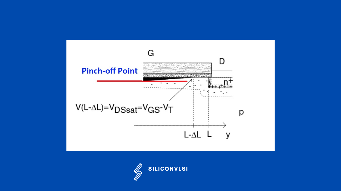
At pinch-off:
- There is no barrier to electron flow.
- Electron concentration is small but not zero.
- The effect of Vds will be less as compared to Vgs on the gate.
- Electrons move fast because the electric field is very high from the drain side.