
Close Menu
  • Analog Design
    • Latest Analog Layout Interview Questions (2025)
  • Digital Design
    • Digital Electronics Interview Question(2025)
    • Top VLSI Interview Questions
  • Physical Design
    • Physical Design Interview Questions for VLSI Engineers
  • Verilog
    • Verilog Interview Questions(2026)
  • Forum
  • Calculators
    • Asynchronous FIFO Depth Calculator
    • Clock Skew and Clock Jitter Calculator
    • Setup Time Calculator
Facebook Instagram YouTube LinkedIn WhatsApp
SiliconvlsiSiliconvlsi
Ask Questions Register in Forum Login in Forum
Facebook Instagram YouTube LinkedIn WhatsApp
  • Analog Design
    • Latest Analog Layout Interview Questions (2025)
  • Digital Design
    • Digital Electronics Interview Question(2025)
    • Top VLSI Interview Questions
  • Physical Design
    • Physical Design Interview Questions for VLSI Engineers
  • Verilog
    • Verilog Interview Questions(2026)
  • Forum
  • Calculators
    • Asynchronous FIFO Depth Calculator
    • Clock Skew and Clock Jitter Calculator
    • Setup Time Calculator
SiliconvlsiSiliconvlsi
Home ยป Why is a P-type (100) substrate doped with boron preferred?
Digital Design

Why is a P-type (100) substrate doped with boron preferred?

siliconvlsiBy siliconvlsiDecember 31, 2023Updated:May 20, 2024No Comments2 Mins Read
Facebook Pinterest LinkedIn Email WhatsApp
Share
Facebook Twitter LinkedIn Pinterest Email

Table of Contents

Toggle
  • P-type (100) Substrate
    • Significance of Epitaxial Growth
    • What are the steps involving N-well diffusion?

P-type (100) Substrate

CMOS integrated circuits start with a P-type (100) substrate heavily doped with boron to minimize substrate resistivity and enhance latch-up immunity. This helps in reducing substrate debiasing, crucial for avoiding CMOS latch-up. The substrate choice is a preventative measure against latch-up, a phenomenon where parasitic structures cause unintended current paths.
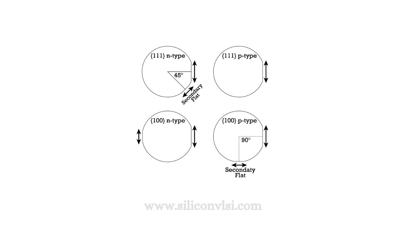
Why are (111)-oriented P-type substrates preferred

Significance of Epitaxial Growth

The initial step involves epitaxial growth, adding a lightly doped P-type epitaxial layer (epi) on the substrate. This thin layer, 5 to 10μm thick, serves as the back gate for NMOS transistors. Unlike standard bipolar processes, CMOS processes do not require buried layers, allowing the use of epi-coated wafers that can be stockpiled for various products. Although epitaxy increases costs, it improves latch-up immunity by enabling the use of a P+ substrate and offers better control over MOS transistor parameters.

What are the steps involving N-well diffusion?

The next step is N-well diffusion, where after thermal oxidation, a patterned photoresist with the N-well mask is used. Ion implantation through oxide windows creates a deep lightly doped N-type region, the N-well. In an N-well CMOS process, NMOS transistors are in the epi, and PMOS transistors reside in the N-well. This process optimizes NMOS transistor performance, slightly degrading PMOS transistor performance due to increased total dopant concentration in the well.

There’s also mention of the P-well CMOS process, where NMOS transistors are in the N-epi, and PMOS transistors are in a P-well. This process optimizes PMOS transistor performance but may face challenges with biasing an N-type substrate in designs with multiple power supplies. The N-well process, chosen for illustration, provides slightly better NMOS transistor performance, a grounded substrate, and compatibility with BiCMOS technology.

Share. Facebook Twitter Pinterest LinkedIn Tumblr Email

Related Posts

Voltage-Aware DRC: 7 Essential Concepts for Reliable Signoff

September 14, 2026

Difference Between Clipper and Clamper

June 22, 2025

What is difference Between RAM Bandwidth and Clock Speed

December 1, 2024
Leave A Reply Cancel Reply

Facebook X (Twitter) Instagram Pinterest Vimeo YouTube
  • About Us
  • Contact Us
  • Privacy Policy
© 2026 Siliconvlsi.

Type above and press Enter to search. Press Esc to cancel.