Close Menu
  • Analog Design
    • Latest Analog Layout Interview Questions (2025)
  • Digital Design
    • Digital Electronics Interview Question(2025)
    • Top VLSI Interview Questions
  • Physical Design
    • Physical Design Interview Questions for VLSI Engineers
  • Verilog
    • Verilog Interview Questions(2024)
  • Forum
Facebook Instagram YouTube LinkedIn WhatsApp
SiliconvlsiSiliconvlsi
Forum Questions Register in Forum Login in Forum
Facebook Instagram YouTube LinkedIn WhatsApp
  • Analog Design
    • Latest Analog Layout Interview Questions (2025)
  • Digital Design
    • Digital Electronics Interview Question(2025)
    • Top VLSI Interview Questions
  • Physical Design
    • Physical Design Interview Questions for VLSI Engineers
  • Verilog
    • Verilog Interview Questions(2024)
  • Forum
SiliconvlsiSiliconvlsi
Home»VLSI Design»Why we extend poly over the diffusion?
VLSI Design

Why we extend poly over the diffusion?

siliconvlsiBy siliconvlsiJanuary 10, 2022Updated:May 12, 2024No Comments1 Min Read
Facebook Pinterest LinkedIn Email WhatsApp
Share
Facebook Twitter LinkedIn Pinterest Email

We extend Poly from the diffusion to avoid the short circuit between the source and drain during fabrication.

During the fabrication process, there are chances that the mask gets a slight misalignment.

OPC(Optical proximity correction)

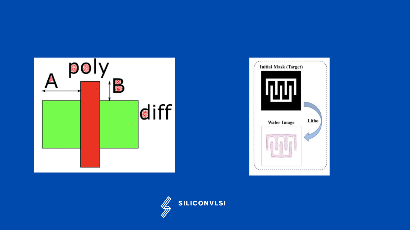
 We all know that we can’t get the exact design in fabrication. there is a reduction or shrink factor in the VLSI Fabrication process(around 1~2%).

 To avoid this corner layout effect, or to improve this shrink factor, we are using OPC(optical proximity correction) based on virtual edge and mask pixelation with a two-phase sampling.

What is the length of diffusion effect in VLSI?

The Length of Diffusion (LOD) refers to the distance from an n-channel or p-channel to the edge of the shallow trench isolation (STI) oxide. Oxide Diffusion (OD) to OD spacing represents the spacing between active areas, known as active-to-active spacing. These factors are part of layout-dependent effects in semiconductor device design.


Share. Facebook Twitter Pinterest LinkedIn Tumblr Email

Related Posts

How Shielding Avoids Crosstalk Problem? What Exactly Happens There?

September 22, 2024

Navigating the Challenges of Gate Dielectric Scaling in MOS Transistors

August 1, 2024

Challenges in Modern SoC Design Verification

April 20, 2024
Leave A Reply Cancel Reply

Facebook X (Twitter) Instagram Pinterest Vimeo YouTube
  • About Us
  • Contact Us
  • Privacy Policy
© 2025 Siliconvlsi.

Type above and press Enter to search. Press Esc to cancel.