
PN junction diode e in Forward bias
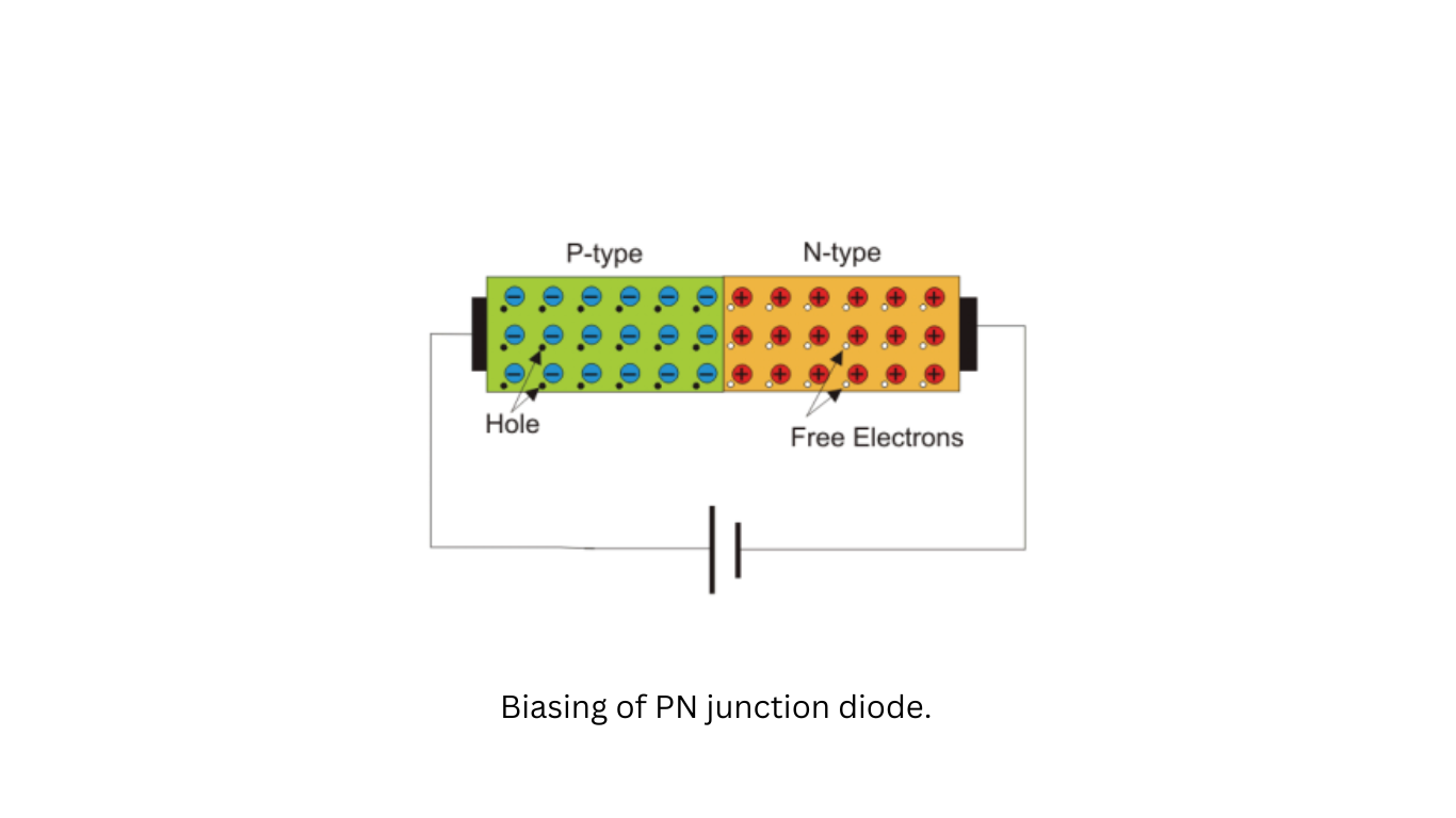
In forward bias, as illustrated in Figure 1, the positive terminal of a voltage source is connected to the p-type side of a diode, and the negative terminal of the source is connected to the n-type side of the diode. When we slowly increase the voltage supplied by this source from zero, the diode enters a forward-biased state.
Initially, there is no current flowing through the diode. This lack of current occurs because, even though an external electric field is applied across the diode, the majority of charge carriers (electrons in the n-type and holes in the p-type) do not experience a strong enough influence from this external field to cross the depletion region. The depletion region, as previously mentioned, acts as a potential barrier that impedes the movement of majority charge carriers. This potential barrier is known as the forward potential barrier.
The majority of charge carriers will begin to cross this forward potential barrier only when the externally applied voltage across the diode exceeds the potential of the forward barrier. For silicon diodes, the forward barrier potential is approximately 0.7 volts, while for germanium diodes, it is about 0.3 volts.
When the externally applied forward voltage across the diode surpasses the forward barrier potential, the free majority charge carriers can cross the barrier, contributing to the forward diode current. In this situation, the diode effectively acts as a short-circuited path, and the magnitude of the forward current is limited only by the externally connected resistors in the circuit.
In summary, forward biasing a diode involves applying a voltage in such a way that it allows the majority of charge carriers to overcome the forward potential barrier, resulting in the diode conducting current in the direction of the external voltage source.
PN junction diode e in Reverse bias
This condition of a diode, where the voltage is applied in reverse, is referred to as the reverse-biased condition, as depicted in Figure 2 In this state, no majority of charge carriers can cross the junction because they are being pushed away from the junction. Therefore, a diode effectively blocks the flow of current when it is reverse-biased.
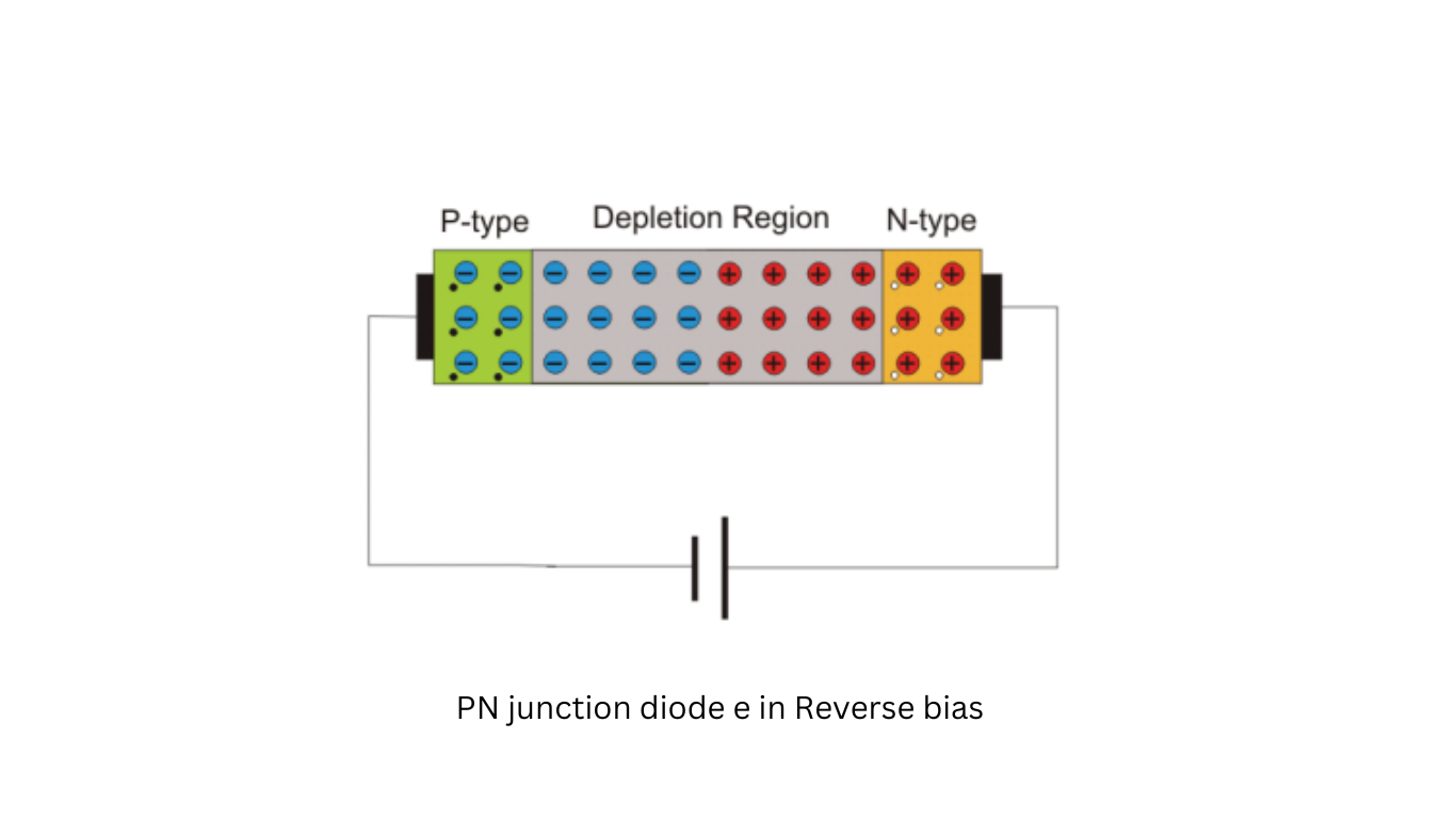
However, there are always some free electrons in the p-type semiconductor and some holes in the n-type semiconductor. These charge carriers with the opposite charge to the majority carriers are called minority charge carriers. In the reverse-biased condition, the holes that find themselves in the n-type side can easily cross the wider, reverse-biased depletion region. The electric field across the depletion region does not hinder them; in fact, it assists minority charge carriers in crossing the region. As a result, there is a small current flowing through the diode from the positive to the negative side. The magnitude of this current is very small because the number of minority charge carriers in the diode is typically very limited. This current is known as the reverse saturation current.
However, if the reverse voltage applied across the diode exceeds a safe value, the electrostatic force and kinetic energy of minority charge carriers can become high enough to break several covalent bonds within the diode. This process generates a large number of free electron-hole pairs in the diode, and this effect can be cumulative. The significant number of generated charge carriers can contribute to a substantial reverse current in the diode. If this current is not limited by an external resistor connected in the diode circuit, it can lead to permanent damage to the diode