What is Analog Layout Design components in VLSI?
Analog Layout remains a time-consuming manual task for most layout designers. Analog Layout devices contain active and passive devices. For as long as integrated circuits have existed, designers have been manually placing individual transistors, drawing every shape and guard ring, and routing every wire by hand.In short, we can say that For Analog layout design we are not using automation for drawing layout
There are two types of Analog Layout devices:
- Active devices
- Passive devices
Active Devices
- Transistors(NMOS & PMOS)
Passive Devices
- Resistors
- Capacitors
- Inductors
Transistor:
- NMOS
NMOS Layout Component: NMOS Bulk terminal is tied to P substrate which is tied with the Ground terminal.

- PMOS
PMOS Layout Component: PMOS Bulk terminal is tied to N-well which is tied with the power terminal.

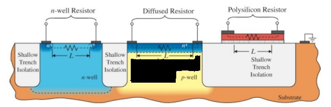
Resistors:
- All materials have some resistivity– Metal layer: 0.1 Ohm/square
– n/p-plus contacts: 10-100 Ohm/square
– n-well: 1000 Ohm/square
– low doped polysilicon: 10 k Ohm/square
How to Matched The Resistor Layout:
We should add Dummy resistors to ensure both resistors have the exact same environment.

Resistor Layout Matching Techniques for Analog layout design
- Use the same material for Resistor
- Use dummy elements at the end of devices from both sides
- Draw the layout in the same orientation
- Put all devices in Close proximity and interdigitate arrayed resistors
- Place resistors in a Low-stress area
- Place resistors away from power devices
Capacitors
There are natural capacitors between each layer of metal, polysilicon or any other related layer. Dielectrics between different metal layers have a thickness of 0.5-1 micron, which gives a rather large area for a given capacitance.

Types of capacitors in the analog layout:
- MIM Capacitor (Metal-Insulator-Metal)
- Poly to Poly Capacitor
- MOM-Capacitors (Metal-Oxide-Metal)
- MOS Capacitor
- Trench Capacitors
What is an Ideal Capacitor?
Ideal Capacitor has the following properties.
- High breakdown voltages
- Low Losses
- Low leakage currents
- High-quality factor (Q)
- Low parasitic capacitance
- Capacitance should be voltage-independent
- High area capacitance
Summary For All Analog Layout Device Matching Techniques.
- Use a Common Centroid layout to reduce linear-gradient errors
- Use unit element arrays
- Use a large Layout area to reduce random error
- Use Interdigitize techniques for matching
- Use of symmetry
- Use a Dummy device for a similar vicinity
- Use Guard rings for isolation and latch-up prevention.
Analog Design Tools
Analog circuit design has evolved significantly from the early days when circuits were developed using hand-drawn schematics and manual calculations. Today, hardware designers have access to various digital tools to facilitate their projects. Schematic CAD (Computer Aided Design) tools enable designers to create schematics from scratch, providing a visual representation of the circuit. Simulation programs play a crucial role in the design process by allowing designers to predict the behavior of the circuit before physical testing. These simulation tools, such as PSpice, LTSpice, Tina-TI, and Multisim, simulate the signal behavior in both time and frequency domains, providing valuable insights to refine and optimize the circuit design.
Why are minimum-sized devices, commonly found in digital circuits, less frequently used in general analog design?
Minimum-sized devices, often used in digital circuits, are less frequently used in general analog design because longer gate lengths are preferred in analog applications. Longer devices are less affected by channel-length modulation, resulting in better performance characteristics.
How can the implant resistance in the source and drain of a MOSFET be reduced in layout design?
The implant resistance in the source and drain of a MOSFET can be reduced in layout design by adding multiple contacts along the width of both the source and the drain. This increased number of contacts lowers resistance, increases current-carrying capability, and more evenly distributes the current load throughout the device.
What advantage does distributing the parasitics into smaller contributions offer in layout design?
Distributing parasitics into smaller contributions, such as by splitting a MOSFET device into parallel devices, offers the advantage of reducing parasitic capacitance and resistance. This reduction improves the overall performance of the device, reduces the impact of parasitics, and allows for better control of electrical characteristics.