
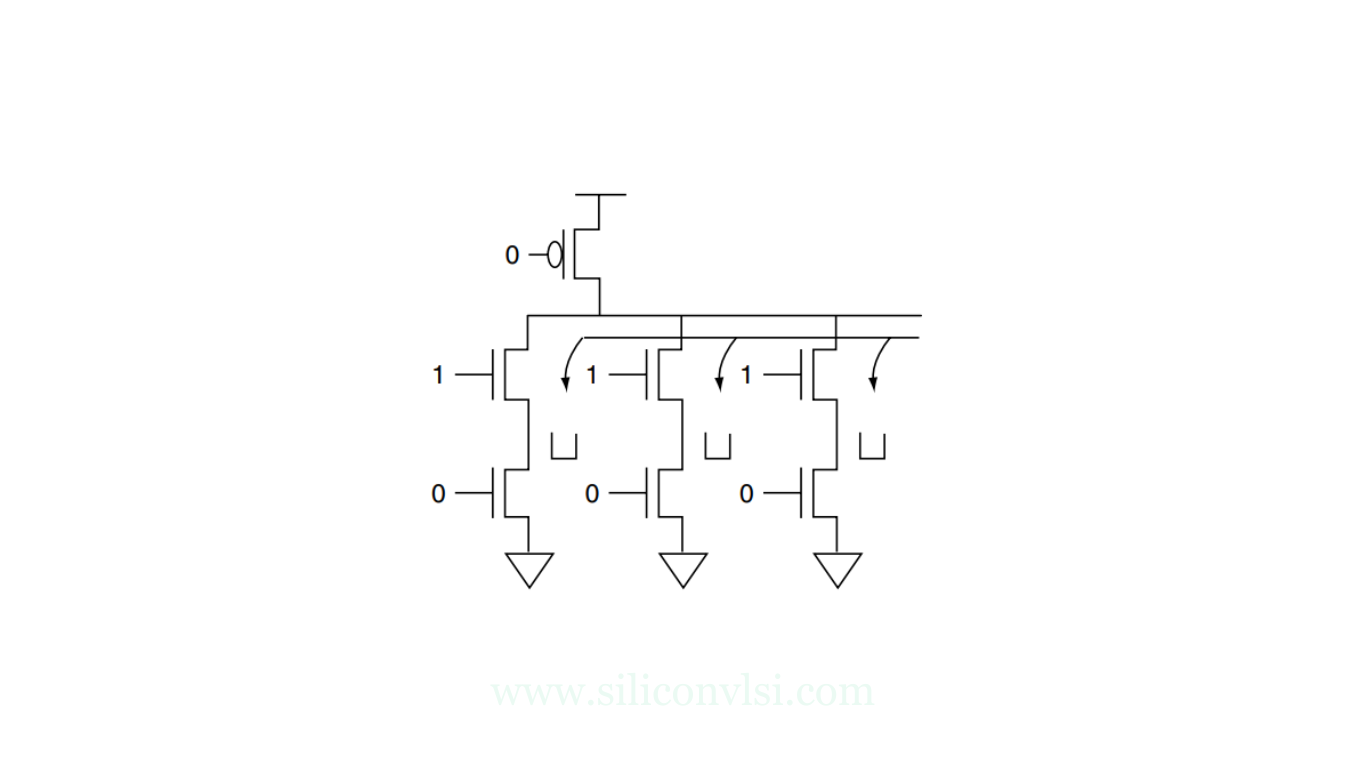
Charge Sharing Noise
Charge-sharing noise arises from charge redistribution between a dynamic evaluation node and intermediate nodes in pull-up or pull-down logic stacks, as shown in Figure 1. This phenomenon primarily affects domino nodes, weakly driven pass-gate latches, and dynamic latches. The ratio of junction capacitance to gate and interconnect capacitance is a crucial technology variable influencing charge-sharing noise. In most circuits, this noise does not exhibit dramatic changes with technology scaling.
Charge Leakage Noise
Charge leakage noise comprises subthreshold conduction in nominally off transistors. This current can either charge/discharge a dynamic node or cause the stable state of a weakly held node to differ significantly from the rails. Charge leakage noise is particularly relevant in wide domino NOR gates, programmable logic arrays (PLA), and memory arrays. The current associated with charge leakage noise rises exponentially with a reduction in threshold voltage, becoming especially significant in deep submicron (DSM) technology. Feedback devices play a crucial role in helping mitigate charge leakage noise.
How does an increased current on power supply lines impact the circuit’s performance?
An increased current on power supply lines causes a rise in IR drop on voltage references, making the gate more sensitive to noise spikes.
What physical design techniques are proposed to address power supply noise in high-speed designs?
Several physical design techniques have been proposed to counter power supply noise in high-speed designs, including
- Sizing up the P/G (power and ground) lines to accommodate large current peaks and minimize IR and L di/dt voltage variations
- Increasing the number of P/G pins
- Deploying decoupling capacitors in the P/G lines
- Performing clock skew scheduling to minimize the number of simultaneous switching. Copper can also be used instead of aluminum to overcome increased resistance in scaled interconnects