

Drain-Induced Barrier Lowering (DIBL) in MOSFET: Effects, Causes & Solutions
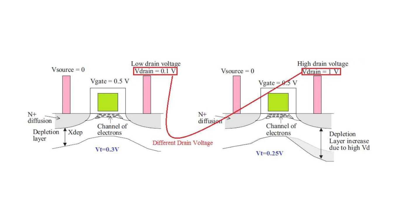
Drain-Induced Barrier Lowering (DIBL) is an important short-channel effect in MOSFETs. It becomes significant when the channel length of a MOSFET is reduced and the electric field produced by the drain begins to strongly influence the channel potential.
In an ideal long-channel MOSFET, the threshold voltage remains nearly independent of the drain-to-source voltage. However, in a short-channel MOSFET, increasing the drain voltage can reduce the effective potential barrier near the source. As a result, the transistor can conduct at a lower gate voltage, causing the threshold voltage (VTH) to decrease.
This reduction in threshold voltage with increasing drain voltage is known as Drain-Induced Barrier Lowering (DIBL).
DIBL becomes increasingly important as transistor dimensions continue to scale because it can increase off-state leakage and make precise transistor control more difficult.
What Is Drain-Induced Barrier Lowering?
Drain-Induced Barrier Lowering is the reduction in the MOSFET’s effective threshold voltage caused by an increase in drain-to-source voltage, particularly in a short-channel device.
Consider an nMOS transistor.
When the drain voltage is increased, the drain depletion region extends further into the channel. In a short-channel device, the drain electric field can significantly influence the potential barrier near the source.
As this barrier is lowered, electrons can enter the channel more easily, even when the gate voltage is relatively low.
Therefore:
Higher VDS → lower energy barrier → lower effective VTH → higher drain current
This effect is much stronger in short-channel MOSFETs than in long-channel MOSFETs.
Why Does DIBL Occur in Short-Channel MOSFETs?
In a long-channel MOSFET, the gate has strong control over the channel, while the drain and source have comparatively less influence over the channel region near the opposite terminal.
When the channel becomes very short, the depletion regions associated with the source and drain occupy a larger fraction of the channel.
As VDS increases, the drain depletion region expands and its electric field penetrates deeper into the channel.
The drain therefore begins to influence the source-channel potential barrier.
This reduces the amount of gate voltage required to establish conduction.
The result is a reduction in the apparent threshold voltage.
Long-Channel MOSFET
For a long-channel device:
- Gate control over the channel is dominant.
- Drain voltage has relatively little influence on VTH.
- DIBL is small or negligible.
Short-Channel MOSFET
For a short-channel device:
- Source and drain depletion regions occupy a larger portion of the channel.
- Drain electric-field influence becomes stronger.
- The source-channel barrier is reduced.
- Effective VTH decreases as VDS increases.
- Subthreshold leakage increases.
Physical Mechanism of DIBL
The physical mechanism of DIBL can be understood by considering the depletion region around the drain.
When the drain voltage increases, the drain-to-body junction becomes more reverse biased. This causes the drain depletion region to expand.
In a short-channel MOSFET, this depletion region can extend significantly toward the source.
The drain electric field then partially controls the channel potential that would otherwise be controlled primarily by the gate.
As the drain field lowers the potential barrier between the source and channel, electrons can move from the source toward the channel more easily.
Consequently, a smaller gate voltage is required to obtain a given drain current.
This appears electrically as a reduction in threshold voltage.
DIBL and Threshold Voltage
One of the most important effects of DIBL is the dependence of threshold voltage on drain voltage.
For an ideal long-channel MOSFET:
VTH ≈ constant as VDS changes
For a short-channel MOSFET affected by DIBL:
VDS ↑ → VTH ↓
This behavior is especially noticeable when the device operates in the subthreshold region.
A lower threshold voltage means that the transistor can conduct more current at a given gate voltage.
Therefore, DIBL can significantly increase the OFF-state current of a transistor.
Effects of Drain-Induced Barrier Lowering
DIBL can affect several important characteristics of a MOSFET.
1. Reduction in Threshold Voltage
The most direct effect is a reduction in the effective threshold voltage as VDS increases.
This makes the transistor easier to turn on.
2. Increase in Subthreshold Leakage
Because the effective threshold voltage decreases, the transistor can conduct more current even when the gate voltage is below the nominal threshold voltage.
Therefore, DIBL contributes to increased subthreshold leakage current.
3. Increase in Static Power
Higher leakage current means that the circuit consumes more power even when the logic is not switching.
This is particularly important in modern low-power and high-density integrated circuits.
4. Loss of Gate Control
DIBL is an indication that the drain is gaining more control over the channel potential.
As transistor dimensions shrink, maintaining strong gate control becomes increasingly important.
5. Degradation of Device Scaling
As channel lengths become smaller, short-channel effects such as DIBL become more pronounced.
Therefore, controlling DIBL is an important consideration in advanced CMOS technology.
DIBL and Subthreshold Leakage
DIBL has a particularly strong effect on the subthreshold region of a MOSFET.
Ideally, when the gate voltage is below VTH, the transistor should be OFF. However, a small amount of subthreshold current still flows.
When DIBL lowers the effective threshold voltage, the subthreshold current increases.
A simplified relationship is:
Higher VDS → lower VTH → higher subthreshold current
This is one reason why short-channel MOSFETs can have substantially higher leakage than their long-channel counterparts.
DIBL as a Short-Channel Effect
DIBL is one of several short-channel effects that become important when MOSFET dimensions are reduced.
Common short-channel effects include:
- Drain-Induced Barrier Lowering (DIBL)
- Threshold-voltage roll-off
- Subthreshold leakage
- Channel-length modulation
- Punch-through
- Hot-carrier effects
- Velocity saturation
These effects arise because the source, drain, gate, and body electric fields interact more strongly as the channel dimensions become smaller.
What Causes DIBL?
Several factors can increase the severity of DIBL.
Shorter Channel Length
DIBL becomes stronger as the channel length decreases.
When the channel is short, the drain depletion region can extend farther toward the source and exert stronger electrostatic control over the channel.
Higher Drain Voltage
Increasing VDS increases the electric field near the drain.
This strengthens the drain’s influence on the channel potential and can further lower the source-channel barrier.
Poor Electrostatic Gate Control
If the gate does not adequately control the channel potential, the drain field can have a greater influence on the channel.
This is why modern transistor structures focus heavily on improving electrostatic control.
Device and Process Parameters
Doping profiles, gate-oxide properties, junction structure, channel dimensions, and transistor architecture can all affect DIBL.
How Can DIBL Be Reduced?
Several device-engineering techniques can be used to reduce DIBL.
1. Increase Channel Doping
Increasing the appropriate channel/body doping can help control the depletion region and reduce the penetration of the drain electric field.
However, excessive doping can introduce other problems, such as mobility degradation and increased variability.
Therefore, doping must be carefully optimized.
2. Use Halo or Pocket Doping
Halo doping, also called pocket implantation, introduces additional doping near the source and drain regions.
It helps control the depletion regions and improves the electrostatic control of the channel.
Halo implants can therefore reduce short-channel effects such as DIBL and threshold-voltage roll-off.
3. Reduce Channel Length Scaling
A longer channel generally provides better immunity to DIBL.
However, increasing channel length can reduce transistor density and performance, so it is not always a practical solution for highly scaled designs.
4. Improve Gate Control
Improving the electrostatic control of the channel is one of the most effective ways to suppress DIBL.
This is a major reason why advanced transistor architectures such as FinFETs and gate-all-around (GAA) devices provide better short-channel control than traditional planar MOSFETs.
5. Optimize Gate-Dielectric and Device Dimensions
Gate dielectric thickness and device geometry influence how effectively the gate controls the channel.
A thinner effective gate dielectric can improve gate control, but dielectric scaling must be carefully engineered to avoid excessive gate leakage and reliability problems.
Therefore, DIBL reduction is not simply a matter of making the oxide thinner; it is part of a broader device-electrostatics optimization problem.
DIBL vs Channel-Length Modulation
DIBL and Channel-Length Modulation (CLM) are related to short-channel behavior, but they describe different effects.
Channel-Length Modulation
In channel-length modulation, increasing VDS causes the drain depletion region to extend into the channel.
This reduces the effective channel length.
The reduction in channel length causes the drain current to increase even after the MOSFET has entered saturation.
Therefore, CLM is primarily associated with the dependence of saturation drain current on VDS.
Drain-Induced Barrier Lowering
In DIBL, the drain electric field lowers the potential barrier near the source in a short-channel MOSFET.
This causes the effective threshold voltage to decrease as VDS increases.
Therefore:
CLM → effective channel length decreases → saturation current increases
DIBL → source-channel barrier decreases → effective VTH decreases
Although both effects involve the drain depletion region and become more significant in short-channel devices, their electrical manifestations are different.
DIBL vs CLM: Comparison
| Parameter | DIBL | Channel-Length Modulation |
|---|---|---|
| Full form | Drain-Induced Barrier Lowering | Channel-Length Modulation |
| Main effect | Reduces effective VTH | Reduces effective channel length |
| Important region | Particularly noticeable in subthreshold operation | Mainly observed in saturation |
| Effect of higher VDS | VTH decreases | ID increases |
| Main consequence | Higher leakage current | Higher saturation current |
| Associated with | Short-channel electrostatics | Drain depletion region extending into channel |
How Is DIBL Measured?
DIBL is commonly extracted from the change in threshold voltage measured at two different drain voltages.
A simplified expression is:
DIBL = −ΔVTH / ΔVDS
For example, suppose the threshold voltage is measured at two drain voltages:
- VDS1 = 0.05 V
- VDS2 = 1.0 V
If the extracted threshold voltage decreases from 0.50 V to 0.40 V, then:
DIBL = −(0.40 − 0.50) / (1.0 − 0.05)
DIBL ≈ 105 mV/V
The exact extraction method and threshold-voltage definition can vary depending on the technology and measurement methodology.
DIBL is commonly reported in units of:
mV/V
A lower DIBL value generally indicates better electrostatic control of the channel.
Why Is DIBL Important in Modern CMOS?
As transistor dimensions shrink, controlling the channel using the gate becomes increasingly difficult.
The drain and source electric fields begin to influence a larger fraction of the channel, making short-channel effects more important.
DIBL can lead to:
- Higher OFF-state leakage
- Increased static power
- Reduced effective threshold voltage
- Greater sensitivity to drain voltage
- Difficulty maintaining predictable transistor behavior
- Increased challenges in low-power circuit design
For this reason, controlling DIBL is an important objective in modern CMOS device design.
DIBL in Advanced MOSFET Structures
Modern transistor architectures are designed to improve gate control and reduce short-channel effects.
Planar MOSFETs have relatively limited electrostatic control as dimensions become extremely small.
FinFETs improve control by allowing the gate to control multiple surfaces of the channel.
Gate-all-around devices go further by surrounding the channel with the gate, providing stronger electrostatic control.
Improved gate control helps suppress short-channel effects such as DIBL.
Key Takeaways
Drain-Induced Barrier Lowering is an important short-channel effect in MOSFETs.
The main points to remember are:
- DIBL becomes significant as the MOSFET channel becomes shorter.
- Increasing VDS can lower the effective threshold voltage.
- The drain electric field reduces the source-channel potential barrier.
- Lower VTH increases subthreshold leakage.
- DIBL can increase static power consumption.
- Halo/pocket doping can help reduce DIBL.
- Improved gate electrostatic control can significantly suppress DIBL.
- DIBL is different from channel-length modulation.
- DIBL is commonly measured in mV/V from the change in VTH with VDS.
- Advanced transistor structures such as FinFETs and GAA devices provide improved control of short-channel effects.
In simple terms:
Higher VDS → stronger drain electric field → lower source-channel barrier → lower effective VTH → higher leakage current.
Understanding DIBL is essential for analyzing the behavior, leakage, scaling, and reliability of modern CMOS devices.