

Channel Length Modulation
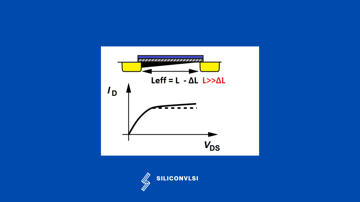
Channel-length modulation arises from the shortening of the effective channel length of the transistor because of the increase in the drain depletion region as the drain voltage is increased. The resulting channel length is simply equal to the metallurgical channel length minus the source and drain
channel length modulation expression
Because of channel-length modulation, the saturation-region drain current will rise somewhat in response to an increase in the drain-to-source voltage. For FETs with channel lengths larger than, say, 2 µm, this modified drain-current formula is a first-order approximation that is reasonably correct.
 depletion region widths. The channel length is another parameter that influences the threshold voltage. For very short channels, the depletion regions of the drain and source junctions are dominant. So overall channel length becomes small Turning the transistor on becomes easier, thus causing a reduction in the threshold voltage.
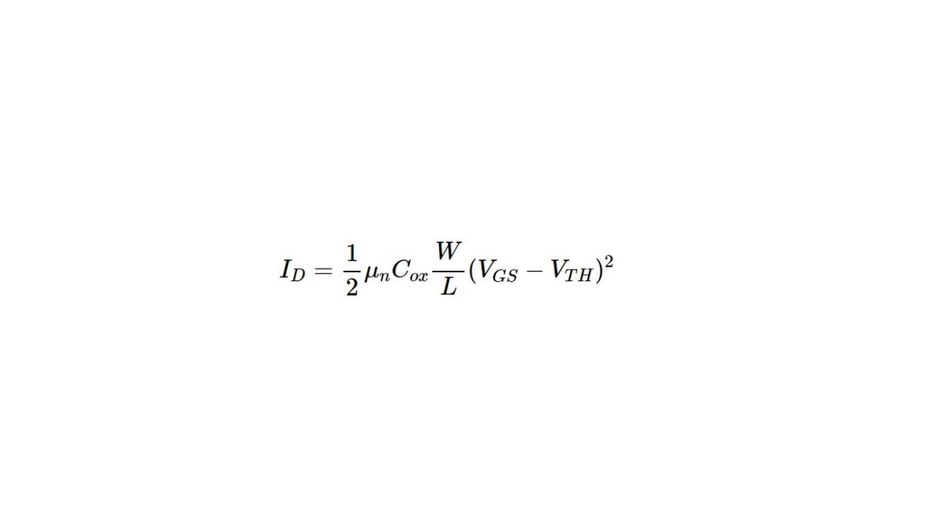
In a triode, the gate-to-source voltage is high enough to permit current flow from the drain to the source, and because of the way the induced channel is constructed. Gate-to-source voltage and drain-to-source voltage have an impact on the drain current’s size.
The triode zone changes into the saturation region as the drain-to-source voltage rises, at which point the only factors affecting the drain current are the physical properties of the FET and the gate-to-source voltage. The following formula represents the gate-to-source voltage (VGS) and drains current (ID) saturation-region relationship.
The transition to saturation mode occurs because the channel gets “pinched off” at the drain end because of Vds=Vds(sat)
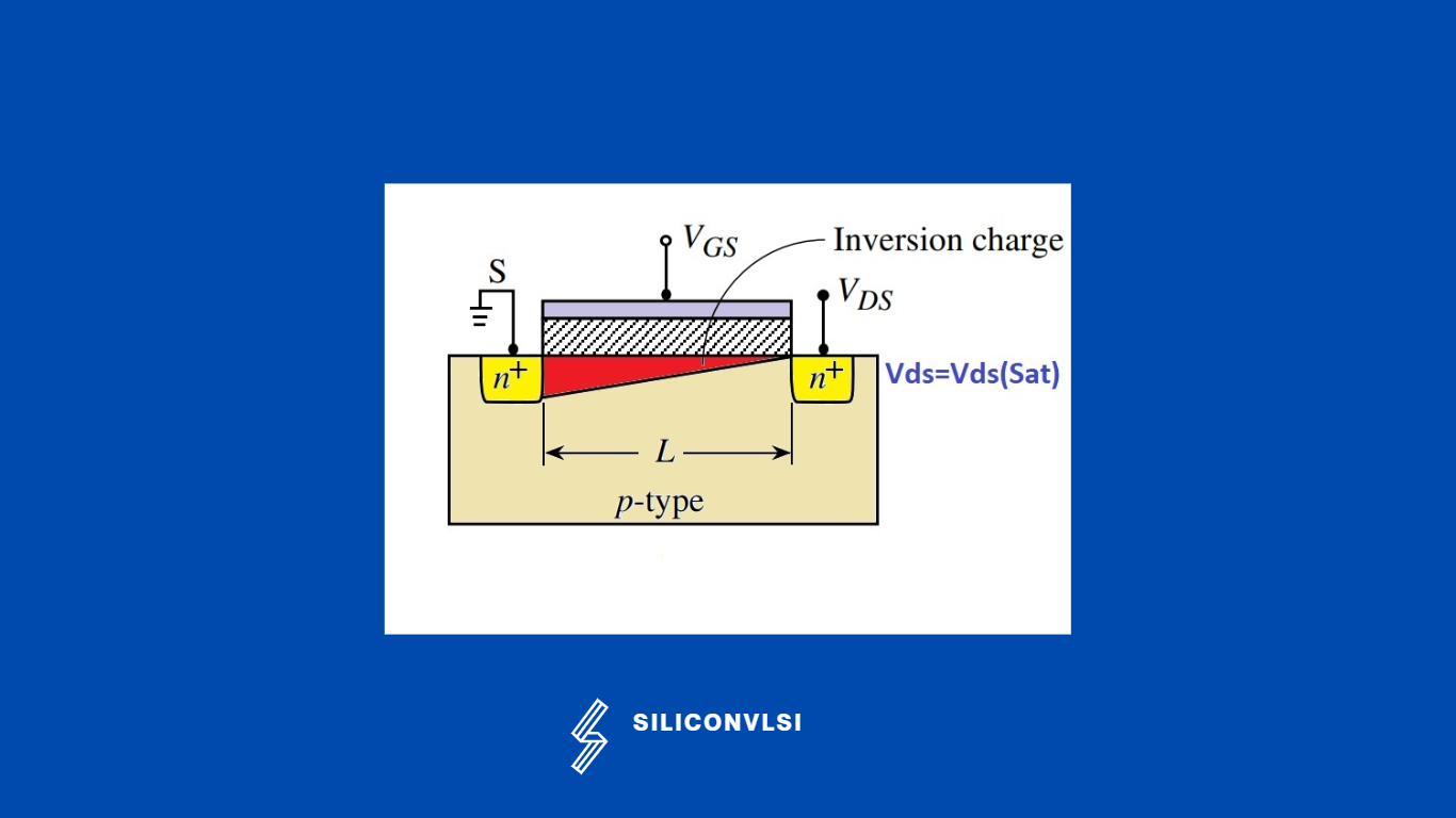
Now if We increase further Vds at the drain not, the channel will start to move further towards the source region, and the Id will be constant because of the High electric field and depletion region.
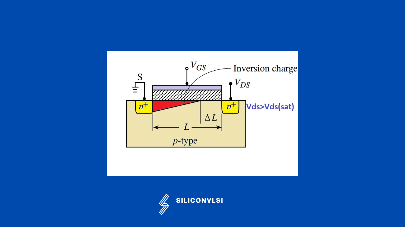
Channel length Modulation Current Equation
The actual channel length will become Leff= L -DeltaL
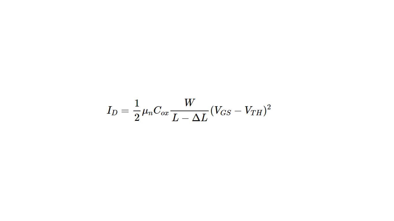
The ratio of the channel’s width toward its length determines the resistance; decreasing the length results in lower resistance and, consequently, higher current flow. The saturation-region drain current will therefore increase slightly as the drain-to-source voltage rises due to channel-length modulation.
As a result, we must adjust the saturation-region drain-current expression to take channel-length modulation into account. To do this, we modify the first statement to include the progressive channel-length reduction
Long Channel and Short Channel device
In the Long channel device, channel length modulation is not more significant, because in Leff= L – ΔL, ΔL is very small, as compared to L.
In the Short Channel device, channel length modulation is more significant, because in Leff= L – ΔL, ΔL is and L has not much difference.
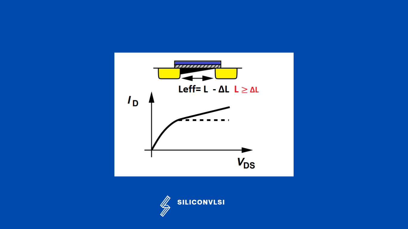
Generally, Short Channel devices are not used in Analog Layouts because of channel length modulation.
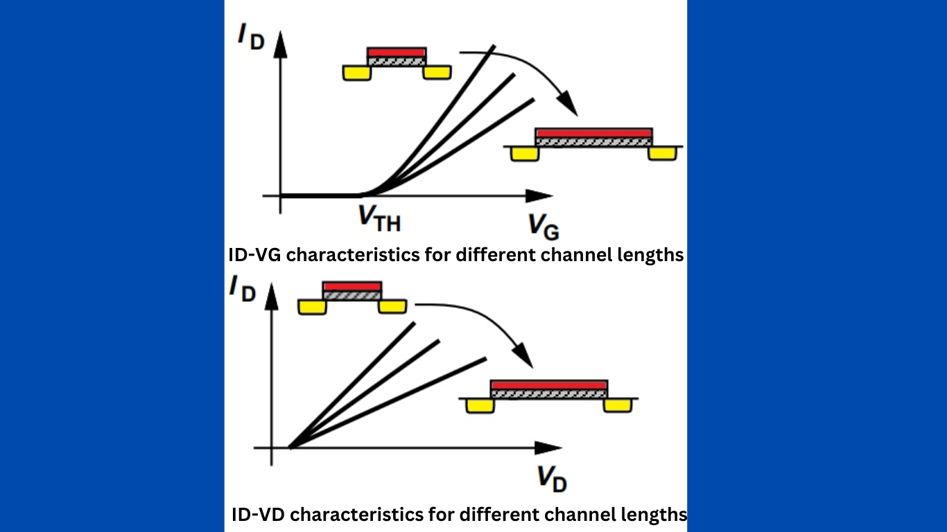
Characteristics for different channel lengths
As the channel length increases, for VG > VT H, the drain current begins with lesser values as the channel length increases, Similarly, ID exhibits a smaller slope as a function of VD. It is therefore desirable to minimize the channel length so as to achieve large drain currents—an important trend in MOS technology development.
What is punch-through?
When the channel length is very small, punch-through occurs. Below this scenario, the source and drain depletion areas might touch, which would cause the drain current to significantly increase.
The punch-through condition’s origin can be understood in light of the following. The source and drain areas of an n-channel device are both doped n+, while the bulk of the device is p-type. Thus, n+-p junctions are formed between the source and drain regions. For a drain current to flow in the device, the drain must be positively biassed. A noticeable depletion area forms at the junction as a result of the drain n+-p junction being reverse-biased.
Frequently Asked Questions
What is Channel Length Modulation?
Channel Length Modulation is the reduction in the effective MOSFET channel length as the drain depletion region expands with increasing drain voltage in saturation.
Why does drain current increase in saturation?
In a practical MOSFET, increasing VDS after saturation causes the effective channel length to decrease. Since drain current depends on the effective W/L ratio, the current increases slightly.
What is the CLM equation?
A commonly used first-order model is:
ID = ½ μCox(W/L)(VGS − VTH)²(1 + λVDS)
for an NMOS in saturation.
What does λ represent?
λ is the Channel Length Modulation parameter. It indicates how strongly the saturation-region drain current changes with VDS.
Does CLM affect output resistance?
Yes. CLM produces a finite output resistance. A commonly used approximation is:
ro ≈ 1/(λID)
Is CLM more significant in short-channel MOSFETs?
Generally, the relative impact can become stronger as channel length decreases, although modern short-channel devices also exhibit other effects that interact with the simple CLM model.
Is CLM the same as DIBL?
No.
CLM describes the reduction of effective channel length and resulting increase in saturation current with VDS, while DIBL describes drain-voltage-induced lowering of the source-channel barrier and threshold voltage.
Is pinch-off the same as Channel Length Modulation?
No. Pinch-off marks the onset of saturation, while Channel Length Modulation describes the subsequent reduction in effective channel length as VDS increases further.
What is punch-through?
Punch-through is a short-channel effect in which source and drain depletion regions extend sufficiently toward each other to significantly weaken channel control and cause excessive current.
Key Takeaways
- Channel Length Modulation causes the effective MOSFET channel length to decrease as VDS increases in saturation.
-
The effective channel length can be represented as:
Leff = L − ΔL
- Because the effective channel becomes shorter, the saturation-region drain current increases with VDS.
-
The first-order CLM equation includes the term:
(1 + λVDS)
- λ represents the Channel Length Modulation parameter.
- CLM gives the MOSFET a finite output resistance.
- Stronger CLM can reduce the voltage gain of analog amplifiers.
- Longer channel devices are often useful when high output resistance and gain are important.
- CLM, DIBL, pinch-off, and punch-through are different physical effects.
- Punch-through becomes a concern when source and drain depletion regions strongly interact in very short-channel devices.
- Understanding this effect is essential for MOSFET modeling, analog VLSI, current mirrors, amplifiers, and transistor sizing.