Close Menu
  • Analog Design
    • Latest Analog Layout Interview Questions (2025)
  • Digital Design
    • Digital Electronics Interview Question(2025)
    • Top VLSI Interview Questions
  • Physical Design
    • Physical Design Interview Questions for VLSI Engineers
  • Verilog
    • Verilog Interview Questions(2024)
  • Forum
Facebook Instagram YouTube LinkedIn WhatsApp
SiliconvlsiSiliconvlsi
Forum Questions Register in Forum Login in Forum
Facebook Instagram YouTube LinkedIn WhatsApp
  • Analog Design
    • Latest Analog Layout Interview Questions (2025)
  • Digital Design
    • Digital Electronics Interview Question(2025)
    • Top VLSI Interview Questions
  • Physical Design
    • Physical Design Interview Questions for VLSI Engineers
  • Verilog
    • Verilog Interview Questions(2024)
  • Forum
SiliconvlsiSiliconvlsi
Home»VLSI Design»Drain Induced Barrier owering (DIBL) effect
VLSI Design

Drain Induced Barrier owering (DIBL) effect

siliconvlsiBy siliconvlsiApril 1, 2022Updated:May 19, 2024No Comments2 Mins Read
Facebook Pinterest LinkedIn Email WhatsApp
Share
Facebook Twitter LinkedIn Pinterest Email

Drain Induced Barrier Lowering (DIBL)

“Drain ­induced barrier lowering (DIBL) effect which causes a reduction in the threshold voltage as the channel length decreases”

DIBL(Drain ­induced barrier lowering) effect occurs when the barrier height for channel carriers at the edge of the source reduces due to the influence of the drain electric field, upon application of a high drain voltage. This increases the number of carriers injected into the channel from the source leading to an increased drain off­current. DIBL(Drain ­induced barrier lowering) effect is also called Short­channel effects (SCE).

Drain ­induced barrier lowering

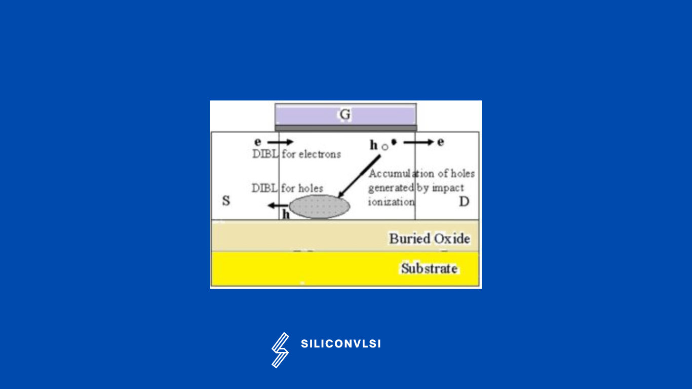
Holes generated near the drain due to impact ionization accumulate in the body region, and then positively bias the body, reducing Vt. This positive bias effect leads to Vt lowering for all gate lengths, including rather long gates such as 2 μm. The Hole generation rate due to impact ionization increases as gate length decreases under a fixed value of Vt.

The DIBL(Drain ­induced barrier lowering) effect on the barrier height for holes reduces the positive bias effect on the body because the accumulated holes in the body can more easily surmount the barrier and flow to the source. As a result, fewer accumulated holes remain which weakens the VT lowering. The potential near the bottom in the thin ­film increases as gate length decreases due to the drain electric field. This leads to the lowering of the barrier height for holes at the source edge near the bottom with shorter gate lengths.

Drain ­induced barrier lowering mechanism

Drain ­induced barrier lowering mechanism with shorter gate lengths, the barrier height for holes near the bottom is lowered by the influence of the drain electric field, and holes accumulated in the body region can more easily flow into the source


Share. Facebook Twitter Pinterest LinkedIn Tumblr Email

Related Posts

How Shielding Avoids Crosstalk Problem? What Exactly Happens There?

September 22, 2024

Navigating the Challenges of Gate Dielectric Scaling in MOS Transistors

August 1, 2024

Challenges in Modern SoC Design Verification

April 20, 2024
Leave A Reply Cancel Reply

Facebook X (Twitter) Instagram Pinterest Vimeo YouTube
  • About Us
  • Contact Us
  • Privacy Policy
© 2025 Siliconvlsi.

Type above and press Enter to search. Press Esc to cancel.