Stages of Physical Design
The physical design process involves several stages that transform a high-level description of a digital circuit into a detailed layout ready for manufacturing. Here’s a brief explanation of each of the six stages of physical design:

Import Design
In this initial stage, the design process begins with the import of design data. This includes taking the RTL (Register-Transfer Level) code or synthesized netlist generated during logic synthesis and using it as the starting point for the physical design. The design tool reads all relevant input files and uses this information to proceed with the physical design process.
Floorplan
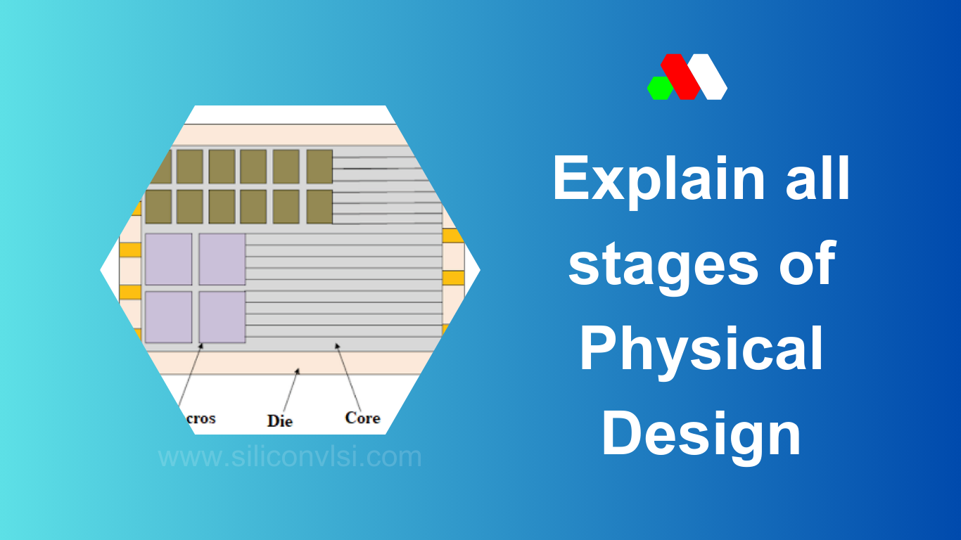
The floorplan stage involves crucial decisions about how to lay out the components on the chip or core. It determines the physical placement of macros (large functional blocks), creates the power grid, and defines the placement of input and output (I/O) pins or pads. Floorplanning establishes the overall chip size and allocates space for various components, ensuring efficient routing areas and power distribution.
Placement
Placement is the process of automatically assigning specific positions to individual standard cells within the chip area defined by the floor plan. This stage ensures that standard cells do not overlap and are optimally positioned to meet design goals. Placement can be divided into global placement, which roughly places cells, and detailed placement, which fine-tunes their positions to adhere to site rows (legalization). Congestion analysis is performed to assess and mitigate routing congestion issues.
Clock Tree Synthesis
The clock tree synthesis (CTS) stage focuses on building a clock distribution network within the chip. It involves the insertion of clock buffers and inverters to balance clock skew and minimize clock insertion delays. A well-optimized clock tree ensures that clock signals reach all flip-flops efficiently, meeting timing requirements and minimizing power consumption.
Routing
Routing is a critical step where logical connections between various components, such as macros, standard cells, and I/O ports, are physically implemented using metal layers. It encompasses two main phases: global routing and detailed routing. Global routing determines which metal layers are used for routing different signals, while detailed routing completes the physical connections. This stage is essential for ensuring signal integrity and meeting timing constraints.
Signoff
The signoff stage is the final step before tape-out, where the physical layout of the chip is reviewed, validated, and tested for quality and performance. It involves running a series of checks and tests, including design rule checks (DRC), layout versus schematic (LVS) checks, and extraction to verify that the design adheres to manufacturing requirements and accurately reflects the intended functionality. Once all signoff checks pass, the design is considered ready for fabrication.
These six stages together form the comprehensive process of physical design, ensuring that a digital circuit design is translated into a manufacturable layout that meets performance, power, and area requirements. The goal is to create a high-quality chip design that functions correctly and efficiently when manufactured.