
PVT
The relationship between propagation delay and IC performance is influenced by various factors, including process (P), voltage (V), and temperature (T), collectively referred to as PVT or PTV conditions. These conditions have a direct impact on how quickly signals can propagate through ICs.
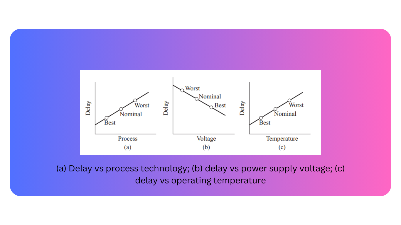
Process Variation
When ICs are manufactured using a specific technology node, they are designed with target dimensions. For example, in a 180 nm technology node, transistors are intended to have a gate length of 180 nm. However, due to inherent process variations during manufacturing, the fabricated transistors do not all have the exact same gate length. Instead, there is typically a Gaussian distribution of dimensions, with the mean being the target gate length. Transistors with shorter gate lengths tend to be faster, while those with longer gate lengths are slower.
Voltage Variation
The supply voltage (V) plays a critical role in determining propagation delay. As the supply voltage increases, the delay through IC devices decreases, resulting in faster operation. Conversely, reducing the supply voltage can increase propagation delay and reduce power consumption.
Temperature Variation
Operating temperature (T) also affects propagation delay. Higher temperatures can lead to increased delay through IC devices. This temperature-dependent delay is a critical consideration for ICs operating in environments with varying temperature conditions.
Optimizing IC design involves a delicate balance among three key parameters: area, speed, and power consumption. Achieving the best possible performance in all three areas simultaneously is often challenging, as these parameters are interrelated. For instance:
Reducing chip area often comes at the expense of increased delay, as more compact designs may require intricate routing that introduces additional delays.
Maximizing speed might necessitate sacrificing chip area and potentially increasing power consumption, especially when higher voltages are used.
Minimizing power consumption can lead to slower operation or require more chip area to implement power-efficient designs.
In summary, IC performance is fundamentally tied to propagation delay, which can be influenced by process variations, voltage levels, and operating temperatures. Designers must carefully balance trade-offs between area, speed, and power to achieve optimal IC performance for a given application. Additionally, as technology nodes advance, interconnect delay has become a critical consideration alongside device delay, further complicating the design process.
Why is it challenging to optimize area, speed, and power simultaneously in IC design, and what trade-offs are typically involved?
Answer: Optimizing area, speed, and power in IC design is challenging because these parameters often have conflicting requirements. It’s difficult to achieve all three simultaneously. For example, reducing the chip area may require a trade-off with an increase in delay, which affects Speed . Similarly, achieving high-speed performance may come at the cost of increased power consumption. Designers must carefully balance these trade-offs based on the specific requirements of the IC and the application it serves.