
Lithography Hotspot Detection Method
Even with all the advancements in resolution enhancement techniques (RETs), lithography hotspots still present a significant challenge in semiconductor manufacturing. In this article, we’ll dive into how these hotspots impact semiconductor manufacturing and explore some advanced techniques you and I can use to tackle this issue.
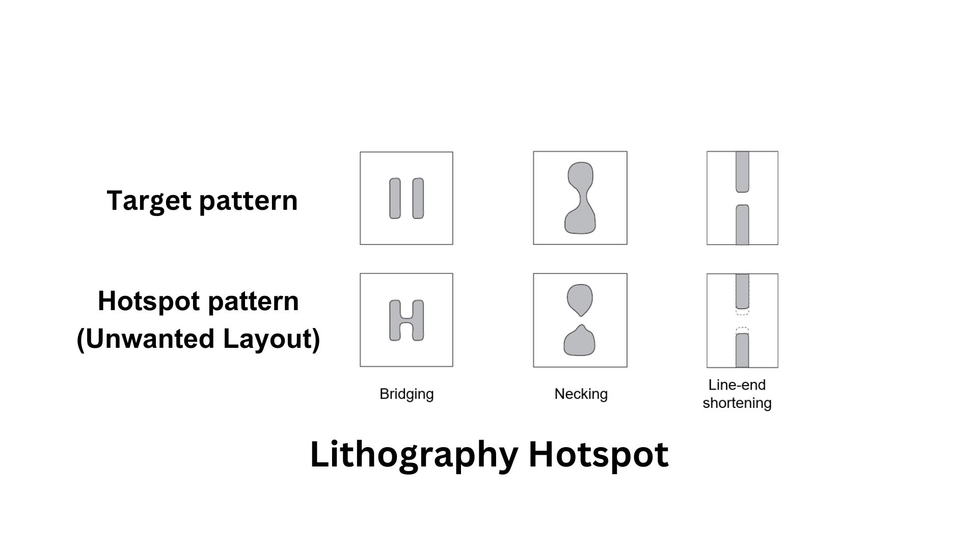
Understanding Lithography Hotspots
What are Lithography Hotspots?
Lithography hotspots refer to regions with poor printability and yield in semiconductor manufacturing processes, especially in deep sub-wavelength processes.
Challenges with Traditional Approaches
Traditionally, lithography simulations were used to identify problematic patterns. However, their computational intensity, particularly for full-chip scale, posed challenges.
Advanced Techniques for Hotspot Detection
Pattern Matching
Pattern matching involves comparing layout patterns with known hotspots stored in a database. This approach enables faster hotspot detection without detailed lithography simulations.
Machine Learning
Machine learning techniques construct regression models based on training data to detect lithography hotspots. These approaches offer promising solutions for full-chip scale hotspot detection.
Hybrid Approaches
Hybrid approaches combining pattern matching and machine learning techniques are also emerging for enhanced accuracy in hotspot detection.
Hotspot Mitigation Strategies
Lithography-Friendly Placement and Routing
Strategies such as lithography-friendly placement and routing aim to minimize interference between adjacent cells and correct hotspots post-routing.
Conclusion
Identifying lithography hotspots is crucial for manufacturing yield. Advanced techniques such as pattern matching and machine learning offer promising solutions for hotspot detection. However, ongoing research is essential to further improve accuracy and integration with evolving lithography technologies.
FAQs (Frequently Asked Questions)
1. How do lithography hotspots impact semiconductor manufacturing?
Lithography hotspots can lead to poor printability and yield, affecting the quality and efficiency of semiconductor manufacturing processes.
2. What are some challenges with traditional hotspot detection methods?
Traditional methods, such as lithography simulations, are computationally intensive, especially for full-chip scale, posing challenges for hotspot identification.
3. How do pattern matching techniques help in hotspot detection?
Pattern matching involves comparing layout patterns with known hotspots stored in a database, enabling faster hotspot detection without detailed lithography simulations.
4. What role does machine learning play in hotspot detection?
Machine learning techniques construct regression models based on training data to detect lithography hotspots, offering promising solutions for full-chip scale hotspot detection.
5. What are some hotspot mitigation strategies discussed in the article?
Hotspot mitigation strategies include lithography-friendly placement and routing, aiming to minimize interference between adjacent cells and correct hotspots post-routing.