
What is a metal layer stack in VLSI? Structure and Importance Explained
In VLSI design, the Metal Layers Stack refers to the multiple layers of metal interconnections used to route signals and power across an integrated circuit (IC). These metal layers are stacked vertically over the silicon substrate, separated by insulating materials, and connected through vias. The number of metal layers can vary based on the technology node and chip complexity, with modern chips using up to 10 or more layers. A well-optimized metal stack is critical for achieving high performance, low power consumption, and reliable signal transmission in semiconductor devices.
Metal Layers in VLSI Physical Design
In electronic design, the utilization of metal layers is important for routing PG/Clock/Signal paths. These metal layers serve as the connections between different points within the design.
The number of metal layers employed for routing can vary depending on the foundry and technology node. For instance, in the 7nm TSMC technology node, 14 metal layers are commonly used, while the 7nm Samsung technology node typically employs 13 metal layers. The specific number of metal layers is determined by factors such as design requirements and congestion considerations.
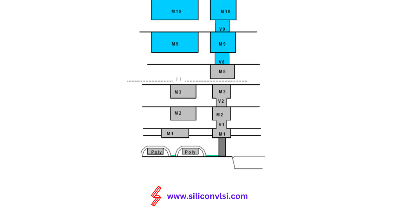
The arrangement of metal layers follows a specific pattern, with horizontal and vertical orientations alternating from M0 to M14. This means that M0 is a horizontal layer, M1 is vertical, M2 is horizontal again, and so on. The purpose behind this horizontal and vertical arrangement is to ensure that the metal layers’ routes are kept separate from one another, reducing the likelihood of congestion and crosstalk issues. We will delve into the details of these considerations in subsequent sections.
To establish connections between the metal layers, VIA structures are employed. These VIA structures serve as bridges that link two adjacent metal layers, facilitating the signal flow throughout the design.
In modern design practices, routing often takes place in a 3-D stack, enabling efficient use of space and improved signal integrity.
It’s worth noting that the resistance value decreases as we progress to higher metal layers. Typically, M1 exhibits around 1.5 times higher resistance than M2, and similarly, M2 demonstrates 1.5 times higher resistance compared to M3, and so forth. This trend allows for better signal propagation and minimizes potential performance limitations.
To better understand how the metal layers are interconnected, let’s examine the accompanying diagram. When two points require connection, the routing tool identifies the shortest path and employs the minimum number of layers necessary to achieve the desired routing objective.
By carefully considering metal layer utilization and optimizing routing strategies, designers can ensure efficient signal transmission and enhance the overall performance of electronic designs.