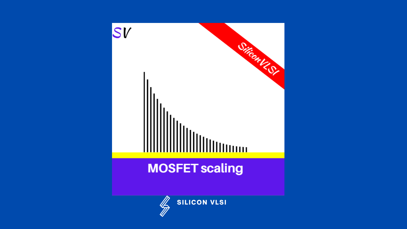
MOSFET Scaling
MOSFET scaling is the reduction in the parameters (like the current, voltage, electric field, etc.) due to the reduction in the length of the transistor with the advancement in technology.
The MOSFET scaling is ultimately limited to the following reasons:
- Lithography.
- Quantum effects.
- Oxide tunneling.
What are the different types of MOSFET scaling?
There are two types of scaling that are common, #
- Constant voltage scaling.
- Constant field scaling.
Constant voltage scaling does not have this problem and is therefore the preferred scaling method since it provides voltage compatibility with older circuit technologies. Constant field scaling yields the largest reduction in the power-delay product of a single transistor. However, it requires a reduction in the power supply voltage as one decreases the minimum feature size.
Advantages and Disadvantages of MOSFET Scaling
Advantages of MOSFET scaling:
- Improvement in speed. #
- Improved ‘throughput’ of the chip.
- Improve the PPA(Power, performance, and Area).
- More transistors can be integrated per chip means in small areas.
- Increase in current, hence improved parasitic capacitance charging time.
- Due to the decrease in channel length L, and hence due to the decrease in transit times.
Disadvantages of MOSFET scaling:
- Complex process technology. #
- More Parasitic effects dominate.
- Suffer from Short channel effects.
Advantages and disadvantages of MOSFET
The term MOSFET in full form is Metal-Oxide-Semiconductor-Field-Effect-Transistor. #
Advantages of MOSFET :
- It can easily to manufacture #
- Require Less area
- Ability to scale down in size
- It is easier to fabricate MOSFET than JFET
- They have high input impedance compared to JFET
- Support high-speed operation compare to JFETs
- It has low power consumption to allow more components per chip surface area
Disadvantages of MOSFET :