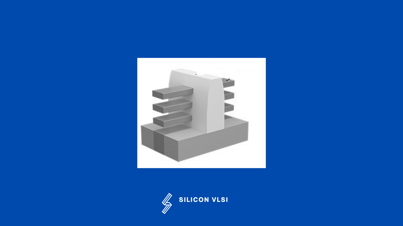
What is Nanosheet FET?
IBM Research has suggested a nanosheet FET as one of the finFET’s replacement technologies. Nanosheet FETs use broader and thicker wires to increase electrostatics and drive current, much like lateral nanowire FETs do. Although they are still in the research and development stage, gate-all-around FETs and nanosheet FETs are two candidates for transistors at single-digit nanometer production nodes.

Why Nanosheet FET?
Now let’s examine finFETs. You must increase the number of fins on the device from one to two to three if you wish to widen it. It’s covert. You stack nanosheets in an active area when using nanosheets. Different device widths can be obtained by varying the nanosheet’s width. This provides you with design flexibility.
You choose a wider sheet if you want transistors or standard cell libraries with a greater and better drive current. You can use a narrow sheet if you want to maximize capacitance and power. This is an additional degree of design flexibility offered by nanosheets.
What are the benefits of gate-all-around (GAA) architecture?
More device width and drive current can be achieved per footprint if a stack of nanosheets is used in place of a single fin. You can observe the change from finFETs to nanosheets for this reason. You may create high-performance 5-track libraries using nanosheets. Another gate-all-around device is nanosheets.
You can scale the gate length a little bit more than with finFETs if you surround the channel with a gate because you obtain much better gate control. Devices with tri-gates are FinFETs. Not all four sides of the channel, but three of them have gates. By increasing the fin pitch, FinFETs have been scaling, going from 14nm to 3nm.
Scaling the fin height will increase device width, whereas scaling the fin pitch will increase the number of fins per footprint. The maximum distance that tall fins can extend is 3 nm. Although you can raise the drive current as the fins go taller, there is a cost in capacitance. It makes no sense to keep increasing the fin height if the increase in drive current is insufficient to compensate for the capacitance cost.
Additionally, it becomes increasingly difficult to wrap the metal and gate dielectric layers around the fins as you make finFET structures taller and the distance between the fins gets smaller owing to fin pitch scaling. So FinFET scaling is becoming more challenging, and for that reason, nanosheets give you a way to get more drive current in the same footprint.
Conclusion
Up to a feature size of 7 nm, FinFET technology has produced a stunning level of performance. The scientific community anticipates that from 7 nm to 5 nm, GAA NW-FETs will replace FinFET technology. The performance of these aforementioned multi-gate devices will be severely hampered by the further reduction of feature size to 3 nm.
In order to get beyond the constraints of the FinFET and GAA NW-FET technologies, the electron device design community must look into alternative device designs such as nanosheet FETs (NS-FETs). The ability of these NS-FETs to scale down even below a feature size of 5 nm with zero short channel effects is what has fueled their development.
Determining the impacts of geometric scaling, substrate material, parasitic channel, temperature, compatibility with various metal gates, and source/drain (S/D) metal depth on NS-FETs has therefore been a major focus of this review study. Due to their exceptional capacity to maintain Moore’s Law, it may be said that vertically stacked NS-FET is the most promising solution for future digital/analog integrated circuit applications.