Optical Proximity Correction (OPC)
Optical Proximity Correction (OPC) plays an important role in improving the accuracy of pattern transfer during lithography. I’ve noticed that OPC effectively addresses optical proximity effects, which become more significant as chip features shrink and are placed closer together.
You might already know that as we aim for higher integration densities in VLSI chips, the physical limits of light diffraction can start to distort the patterns we try to print. This can result in inaccuracies and lower yields. To solve these challenges, we use OPC to adjust the photomask patterns, ensuring that the final patterns on the wafer match the intended design.
How OPC Works
OPC is based on the careful manipulation of mask layouts to compensate for the non-ideal behavior of light during lithography. By introducing controlled modifications to the original design, OPC aims to correct image distortion, improving critical dimension (CD) uniformity and minimizing process variations.
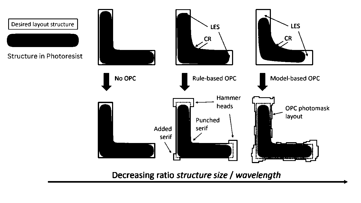
The extent of imaging mistakes grows as the wavelength of light’s feature size decreases. Rule-based OPC is not a viable option in this situation because the exposure-outcome is now more and more influenced by the environment. Then, each structure’s corrections to the photomasks must be determined separately. The methods used here are based on models that explain the effects of waves on light. In the following figure, a model-based OPC’s outcome is depicted.

OPC Methods
There are two primary approaches to OPC:
Rule-Based OPC
Rule-based OPC involves creating predefined sets of rules to modify the mask layout. These rules are based on empirical data and simulations, making it a practical solution for correcting systematic errors. Shown in the above figure.
Model-Based OPC
Model-based OPC, on the other hand, relies on sophisticated mathematical models that simulate the lithographic process. This approach provides greater accuracy and adaptability, making it suitable for correcting complex patterns and reducing random errors. Shown in the above figure.
OPC in VLSI Manufacturing
Resolution Enhancement Techniques (RET)
RET, including OPC, has played a pivotal role in enabling the semiconductor industry to push the limits of Moore’s Law. OPC, combined with other techniques like sub-resolution assist features (SRAFs) and phase-shifting masks, allows for the fabrication of subwavelength features.
OPC Challenges and Solutions
As technology nodes advance, the challenges associated with OPC implementation also increase. Issues such as mask complexity, computational intensity, and hotspot fixing demand innovative solutions. Advanced algorithms and hardware acceleration have addressed these challenges, ensuring timely delivery of error-free masks.
The Future of OPC
With the relentless pursuit of smaller nodes and higher integration densities, OPC continues to be a critical technology in the VLSI domain. Emerging technologies like extreme ultraviolet (EUV) lithography and multiple patterning further accentuate the need for advanced OPC techniques.
Conclusion
In conclusion, Optical Proximity Correction (OPC) plays a pivotal role in modern VLSI manufacturing, enabling the fabrication of intricate semiconductor designs with exceptional accuracy. By compensating for optical proximity effects, OPC ensures high yield and reliable chip functionality. As the semiconductor industry ventures into even smaller nodes, OPC will remain a key enabler in the relentless quest for technological advancement.
FAQs
Why is OPC important in VLSI manufacturing?
OPC is essential in VLSI manufacturing to mitigate the impact of optical proximity errors, ensuring precise and reliable pattern replication.
What are the primary methods of OPC?
The two main approaches to OPC are rule-based OPC and model-based OPC, each with its advantages and use cases.
How does OPC contribute to shrinking feature sizes?
OPC, along with Resolution Enhancement Techniques (RET), enables the fabrication of smaller nodes by compensating for diffraction-limited imaging.
What challenges does OPC face in advanced technology nodes?
Advanced technology nodes bring challenges like increased mask complexity and computational intensity, which are addressed through innovative algorithms and hardware acceleration