

Overshoot and Undershoot Glitch in VLSI: 7 Essential Crosstalk Concepts
In VLSI circuits, overshoot and undershoot glitches are unwanted voltage excursions that can occur because of signal coupling between nearby interconnects.
When a switching signal on one net affects a neighboring net, the switching net is called the aggressor, while the affected net is called the victim.
These effects become increasingly important as interconnect dimensions shrink and signal transitions become faster.
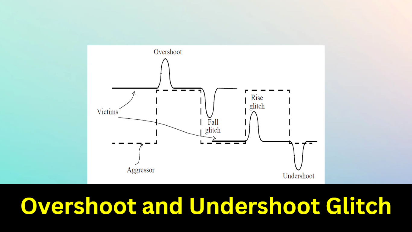
Overshoot and undershoot glitches caused by crosstalk coupling.
What Is an Overshoot Glitch?
An overshoot glitch occurs when the voltage on a victim net temporarily rises above its expected steady-state value.
For example, if a victim signal is expected to remain at logic HIGH, coupling from a nearby switching aggressor can cause its voltage to temporarily exceed the normal HIGH level.
Conceptually:
Expected HIGH → temporary voltage above HIGH → returns to HIGH
This temporary excursion is called an overshoot.
An overshoot does not necessarily mean that the victim logic has changed state. Whether it creates a functional problem depends on its amplitude, duration, receiver threshold, timing, and the technology’s electrical limits.
What Is an Undershoot Glitch?
An undershoot glitch is a temporary voltage excursion below the expected steady-state value.
For example, when a victim net is expected to remain LOW, coupling from a switching neighboring net can temporarily pull the victim voltage below its normal LOW level.
Conceptually:
Expected LOW → temporary voltage below LOW → returns to LOW
This is called an undershoot.
Large undershoot or overshoot events can potentially cause:
- Incorrect logic interpretation
- Timing problems
- Increased device stress
- Substrate or supply noise
- Reliability concerns
What Is Crosstalk Noise?
Crosstalk noise is unwanted electrical coupling between physically adjacent or otherwise coupled signals.
In an integrated circuit, neighboring wires have parasitic coupling capacitance. When the voltage on one wire changes, some of that electrical activity can influence another wire.
The two important terms are:
- Aggressor: the net whose switching activity creates the disturbance.
- Victim: the net that experiences the disturbance.
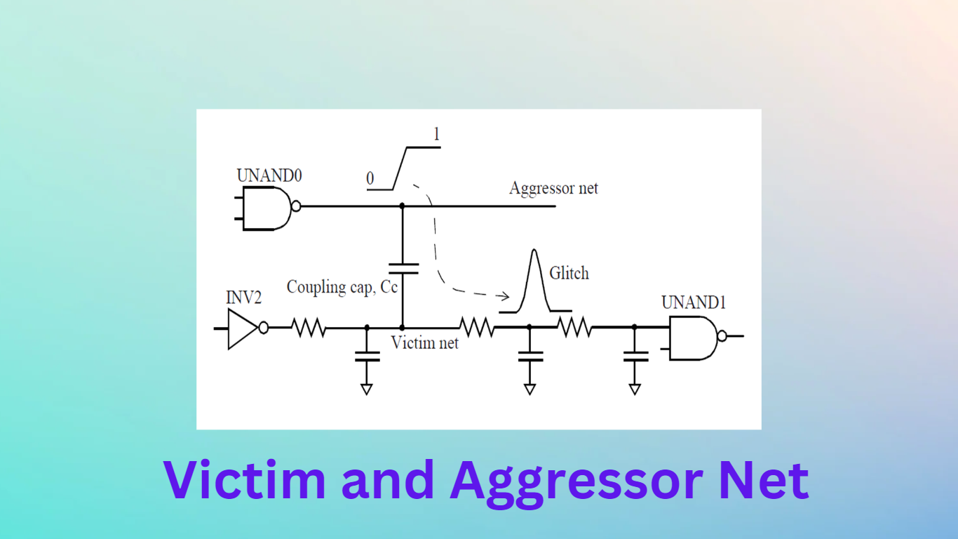
Aggressor and victim nets in a crosstalk scenario.
A simplified capacitive relationship is:
I = C × dV/dt
where:
- I is the transient coupling current,
- C is the coupling capacitance,
- dV/dt represents the aggressor’s voltage-transition rate.
Therefore, a faster aggressor transition can produce a stronger transient disturbance for a given coupling capacitance.
What Causes Noise in VLSI?
Several physical and electrical factors can increase the importance of interconnect noise.
1. Smaller Geometries
As technology scales, wires become closer together. The interaction between neighboring interconnects can therefore become more significant.
2. Higher Routing Density
A highly congested design may contain many parallel wires running close to one another.
Greater proximity can increase coupling.
3. Faster Signal Transitions
Fast rise and fall times increase the rate of voltage change.
A faster transition can produce stronger capacitive coupling effects.
4. Increasing Interconnect Complexity
Modern chips contain enormous numbers of devices and interconnects. As routing becomes more complex, parasitic coupling becomes increasingly important.
5. Metal Stack Characteristics
Metal width, spacing, thickness, dielectric properties, and the relative geometry of adjacent layers all affect parasitic capacitance.
6. Lower Supply Voltages
When supply voltage decreases, the noise margin can also become smaller. A disturbance that might have been insignificant at a higher supply voltage can therefore become more important.
Crosstalk Glitch vs Crosstalk Delay
Crosstalk effects in VLSI physical design are commonly divided into two important categories.
Crosstalk Noise
Crosstalk noise refers primarily to a voltage disturbance on a victim net when the victim is otherwise not undergoing its intended transition.
For example:
Victim = stable
Aggressor = switching
The switching aggressor causes a temporary disturbance on the victim.
Crosstalk Delay
Crosstalk delay occurs when both the victim and aggressor are switching, and the aggressor’s transition changes the timing of the victim transition.
The victim can become either:
- slower than expected, or
- faster than expected.
This distinction is important during static timing analysis (STA).
Types of Crosstalk Glitches
Crosstalk disturbances can appear in different forms depending on the direction and operating condition of the signals.
Common categories include:
- Rise glitch
- Fall glitch
- Overshoot
- Undershoot
The actual waveform depends on the coupling network, driver characteristics, victim capacitance, and switching behavior.
What Determines Glitch Magnitude?
The amplitude of a crosstalk glitch depends on several factors.
Aggressor Slew
A faster aggressor transition generally produces a stronger coupling disturbance.
Coupling Capacitance
Greater coupling capacitance allows more transient interaction between the aggressor and victim.
Therefore:
Higher coupling capacitance → potentially larger crosstalk disturbance
Victim Driving Strength
A strongly driven victim can resist the disturbance more effectively than a weakly driven or floating victim.
Therefore, driver strength is an important factor in crosstalk analysis.
Victim Ground Capacitance
The victim’s capacitance to ground and other surrounding structures affects how much its voltage changes in response to coupled charge.
A larger total victim capacitance generally makes a given injected charge produce a smaller voltage excursion.
Physical Wire Geometry
Crosstalk is also influenced by:
- Parallel run length
- Wire spacing
- Metal dimensions
- Dielectric properties
- Relative layer arrangement
Longer parallel routes can have greater coupling than short neighboring segments.
What Is Crosstalk Delay?
Crosstalk delay is the change in propagation delay of a victim signal caused by switching activity on nearby aggressor nets.
The effect depends primarily on the relative switching directions of the aggressor and victim.
There are two commonly discussed cases:
- Opposite-direction switching
- Same-direction switching
Positive Crosstalk Delay
When the aggressor switches in the opposite direction to the victim, the coupling tends to oppose the victim’s transition.
This can make the victim transition more slowly.
As a result:
Victim transition is delayed → positive crosstalk delay
For example:
- Victim: LOW → HIGH
- Aggressor: HIGH → LOW
The aggressor’s transition can oppose the victim’s transition through capacitive coupling.
The victim therefore requires more time to reach the required logic threshold.
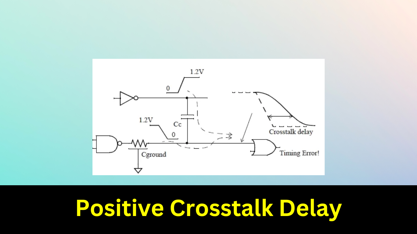
Opposite-direction switching can increase victim delay.
Negative Crosstalk Delay
When the aggressor and victim switch in the same direction, the coupling can assist the victim’s transition.
This can make the victim transition faster.
As a result:
Victim transition is accelerated → negative crosstalk delay
For example:
- Victim: LOW → HIGH
- Aggressor: LOW → HIGH
The aggressor’s transition can assist the victim through capacitive coupling.
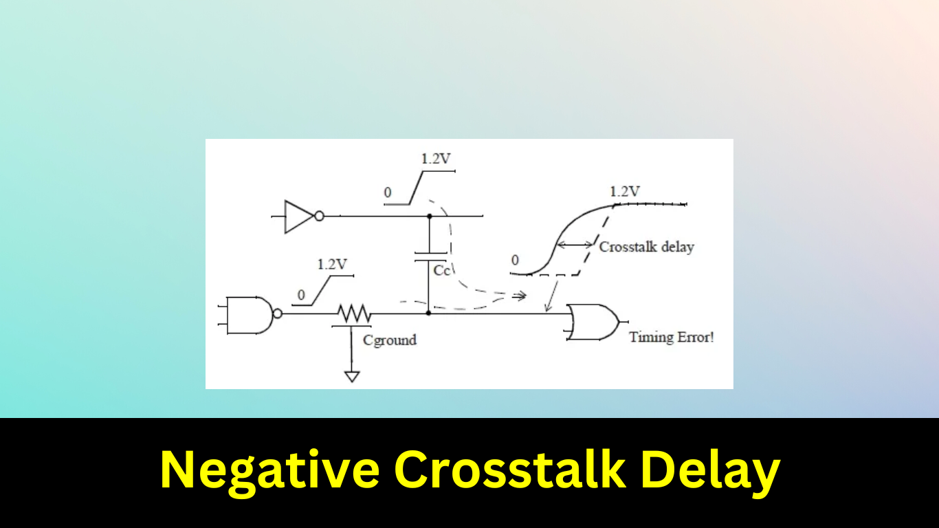
Same-direction switching can reduce victim delay.
Positive vs Negative Crosstalk Delay
| Characteristic | Positive Crosstalk Delay | Negative Crosstalk Delay |
|---|---|---|
| Aggressor direction | Opposite to victim | Same as victim |
| Effect on victim | Opposes transition | Assists transition |
| Victim delay | Increases | Decreases |
| Typical result | Slower transition | Faster transition |
| Timing impact | Can worsen setup timing | Can reduce propagation delay |
The exact amount of delay change depends on the interconnect and driver/receiver characteristics.
Overshoot, Undershoot and Crosstalk Delay
These concepts are related but should not be treated as identical.
| Phenomenon | Victim condition | Main effect |
|---|---|---|
| Crosstalk noise | Victim is relatively stable | Voltage disturbance |
| Overshoot | Victim temporarily exceeds expected upper level | Positive voltage excursion |
| Undershoot | Victim temporarily falls below expected lower level | Negative voltage excursion |
| Positive crosstalk delay | Victim and aggressor switch oppositely | Victim becomes slower |
| Negative crosstalk delay | Victim and aggressor switch in same direction | Victim becomes faster |
This distinction is particularly useful when analyzing post-route timing and signal integrity.
How Can Crosstalk Be Reduced?
Physical-design engineers can reduce unwanted coupling using several techniques.
Increase Wire Spacing
Increasing the distance between neighboring wires can reduce coupling capacitance.
Reduce Parallel Run Length
Avoiding long stretches of parallel routing can reduce the total coupling.
Use Appropriate Metal Layers
Moving a sensitive signal to a different routing layer can sometimes reduce coupling to an aggressor.
Strengthen the Victim Driver
A stronger driver can make the victim less susceptible to voltage disturbances.
Use Shielding
Sensitive nets such as clocks or critical signals may be shielded with appropriate power or ground structures when permitted by the technology and routing methodology.
Optimize Slew
Controlling signal transition characteristics can reduce excessive coupling effects.
Reduce Coupling Capacitance
Physical routing optimization can reduce the parasitic coupling between neighboring nets.
Crosstalk Analysis in VLSI Physical Design
Crosstalk analysis becomes particularly important after routing because the physical geometry of the interconnect is now known.
A simplified flow is:
Placement → CTS → Routing → Parasitic Extraction → Crosstalk Analysis → Timing Signoff
The extracted parasitic information can include:
- Coupling capacitance
- Ground capacitance
- Resistance
- Interconnect delay
Timing-analysis tools can then evaluate how different aggressor switching scenarios affect victim nets.
Why Is Crosstalk Important?
Crosstalk can affect both signal integrity and timing.
A sufficiently large noise pulse can potentially cause a receiver to interpret an incorrect logic level.
Crosstalk-induced delay can also change the timing of a signal path.
Therefore, physical-design engineers need to consider crosstalk during:
- Routing
- Signal-integrity analysis
- Static timing analysis
- Clock implementation
- Power planning
- Signoff
Frequently Asked Questions
What is an overshoot glitch?
An overshoot glitch is a temporary voltage excursion in which a signal rises above its expected steady-state upper value.
What is an undershoot glitch?
An undershoot glitch is a temporary voltage excursion in which a signal falls below its expected steady-state lower value.
What is an aggressor net?
An aggressor is a switching net whose electrical activity causes unwanted coupling onto another net.
What is a victim net?
A victim is the net that experiences the disturbance caused by one or more aggressors.
What causes crosstalk noise?
Crosstalk is primarily caused by parasitic coupling between nearby interconnects, including capacitive coupling and, depending on the physical structure and frequency range, potentially inductive effects.
What is positive crosstalk delay?
Positive crosstalk delay occurs when aggressor activity opposes the victim’s transition, increasing the victim’s propagation delay.
What is negative crosstalk delay?
Negative crosstalk delay occurs when aggressor activity assists the victim’s transition, reducing the victim’s propagation delay.
How can crosstalk be reduced?
Common techniques include increasing wire spacing, reducing parallel run length, optimizing routing layers, controlling slew, strengthening vulnerable drivers, and using shielding where appropriate.
Key Takeaways
- Crosstalk is unwanted coupling between nearby signals.
- The switching signal is called the aggressor.
- The affected signal is called the victim.
- An overshoot takes the victim voltage temporarily above its expected upper level.
- An undershoot takes the victim voltage temporarily below its expected lower level.
- Crosstalk noise primarily describes voltage disturbance.
- Crosstalk delay describes a change in the timing of a switching victim.
- Opposite-direction switching generally produces positive crosstalk delay.
- Same-direction switching generally produces negative crosstalk delay.
- Coupling capacitance, wire spacing, parallel run length, slew, and victim characteristics strongly influence crosstalk.
- Crosstalk analysis is an important part of modern VLSI physical design and timing signoff.