
Power Dissipation in VLSI
Power dissipation occurs when the circuit uses both current and voltage. It is an unavoidable constraint, especially when it comes to portable devices.
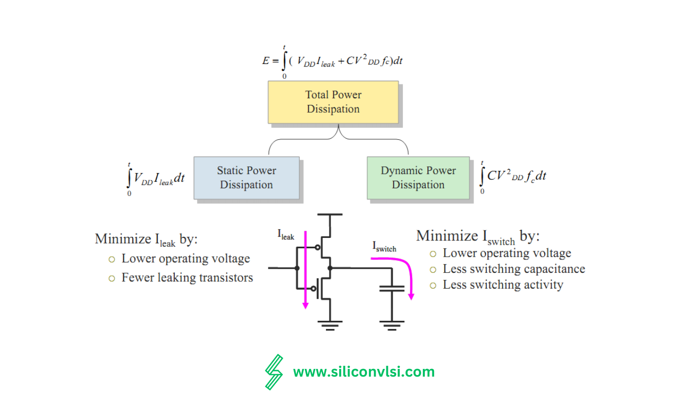
Types of Power Dissipation
Power dissipation in circuits can be categorized into two types:
Static power dissipation: This occurs as leakage current when the system is not powered or in standby mode. Various sources contribute to leakage currents, such as subthreshold leakage, diode leakages, tunnel currents, and gate leakage.
Dynamic power dissipation: This type of power dissipation happens during logic transitions when logic gates charge and discharge load capacitance. It results from the switching activities of transistors.
How to Minimizing Power Dissipation
Minimizing Power Dissipation with Low Power Design VLSI companies can adopt several measures to reduce power dissipation. Here are some ways to implement low-power design:
Reduce supply voltage: Lowering the supply voltage effectively reduces power consumption. A reduction of the supply voltage by a factor of two can result in a four-fold reduction in power consumption. However, reducing the supply voltage also impacts performance, which can be mitigated by scaling down the threshold voltage.
Physical capacitance: Dynamic power consumption depends on the physical capacitance being switched. Besides reducing voltage, lowering capacitance can help achieve lower power dissipation.
Design process: Low-power VLSI design involves optimization at various levels, starting from the system and algorithmic levels to circuit and layout levels.
By implementing these strategies, VLSI companies can reduce power dissipation and enhance the overall efficiency of their designs.
Why is power consumption important in System on Chip (SoC)?
- Power management is important in SoCs for several reasons:
- Costs associated with packaging and cooling.
- Standby time and battery life.
- Digital noise immunity.
- Environmental concerns.