
What is power planning in VLSI?
One of the most important stages in physical design is power planning. It will be utilized to supply power to macros and standard cells while staying under the IR-Drop limit. The resistance of the metal wires that make up the power distribution network causes a steady-state IR Drop. Steady-state IR Drop minimizes the voltage differential between local power and ground, lowering the speed and noise immunity of local cells and macros.
Power planning refers to the process of ensuring that all macros, standard cells, and other components within a design receive adequate power. It is also known as pre-routing because the Power Network Synthesis (PNS) is conducted before the actual signal routing and clock routing take place. Typically, a power ring is designed around the core to facilitate efficient power distribution throughout the design.
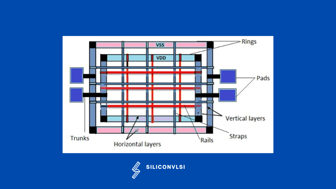
- Rings: Its Carries VDD and VSS around the chip
- Stripes: Its Carries VDD and VSS from Rings across the chip
- Rails: It connects VDD and VSS to the standard cell VDD and VSS.
- Trunk: The connection between Pad and Ring
- Pad: Interface from IC to the outside world.
Power planning involves following things
- Calculating the required number of power pins
- Rings and stripes count
- Ring and striped widths
- IR drop
Why do we do a power plan before the placement of standard cells in Physical design?
Before determining the ideal site for a cell, Place and Route tools will do timing and congestion analyses. If the PG mesh is not present during the placement task, the congestion estimate will be incorrect. That is, even if the placement concludes that there is no congestion. If you want to draw power mesh later, you might not be able to find enough tracks.
So it is always best practice in today’s designs to do all PG routing before starting PnR. It will reduce preroute- post-route correlation issues and provide predictable results.
Power planning is helping to make sure all devices placed will get power. The width and spacing of power straps in each layer are decided depending on the power requirement of the device.
What is VerifyPowerVia/Missing Via/Enough Via check in VLSI?
This checks for any via missing intersection points between the layers, if any via is missing then we need to add vias again or in that specific location, we need to add power via separately. In some companies have this script that will fill automatic vias(Auto Via Check). Make sure there are no routing blockages or any other nets in that region.
Floorplanning and Powerplannig are necessary for Physical design