
Process Variation in VLSI
Process Variation in VLSI is related to PVT(Process Voltage and Temperature). The lateral dimension, doping concentration, and thickness are always subject to change during the production of devices and interconnects. The variances vary from wafer to wafer, from one die to another on the same wafer, and from one die to another. The terms “inter-die” and “intra-die” refer to these variations. These variances ultimately result in changes to the device’s settings, including:
- Channel length
- Oxide thickness
- Threshold voltage
The following modifications are also happening to interconnects.
- Spacing
- Line width
- Contact resistance
- Metal and dielectric thickness
Within a die or wafer, the device characteristics can differ due to process variances. Therefore, this effect must be considered when designing VLSI circuits to ensure consistent performance across all devices manufactured in a batch.
Sources of variation
- Supply voltage (V) #
- Process variation (P)
- Operating Temperature (T)
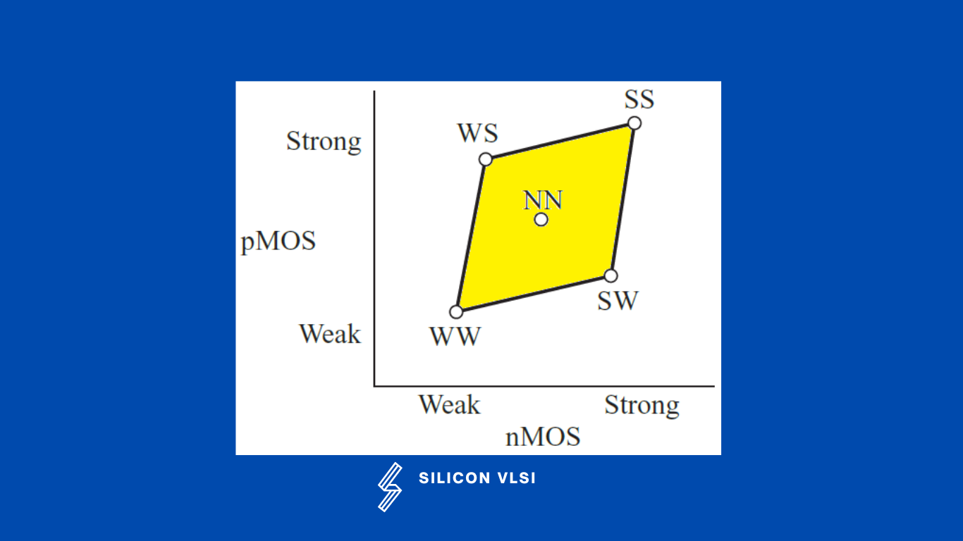
Process Corners in VLSI
The most commonly used design corners are shown in the following figure, The four extreme corners are joined together to form a box within which the circuit is characterized and the performance is ensured. The double letter indicates: #
WW : weak weak corner SW : strong weak corner WS : weak strong corner SS : strong strong corner
The following table describes the best, nominal, and worst timing analysis corners. VDD is assumed to be 1.0 V with a ±10% variation, i.e., 1.1 V and 0.9 V. The operating temperature range is –40°C (low temperature), 27°C (room temperature), and 105°C (high temperature).
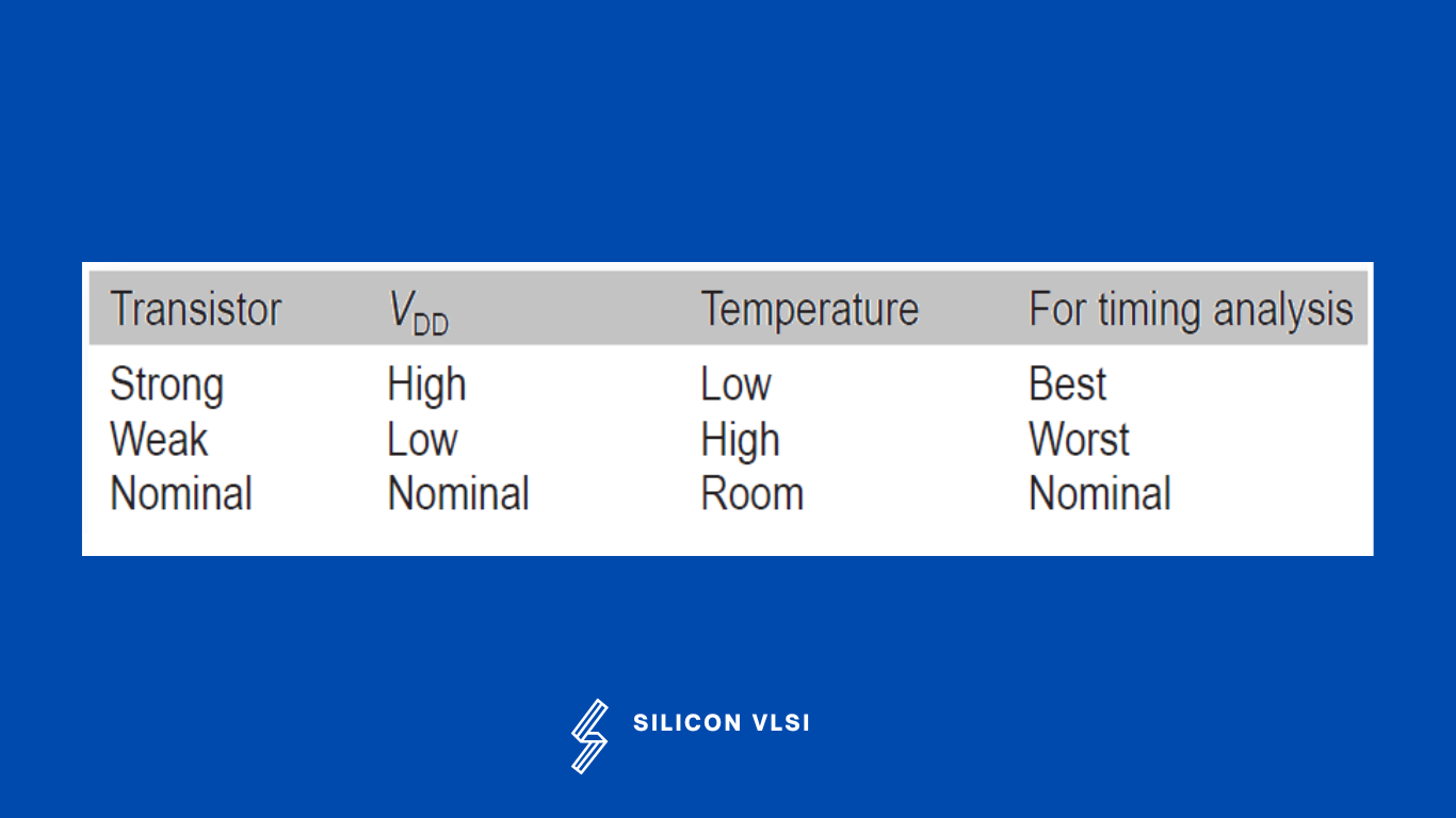
- A combination of a strong transistor, the highest voltage, and the lowest temperature will produce the least delay through a circuit,
- A combination of a weak transistor, the lowest voltage, and the highest temperature will produce the highest delay through a circuit.
- A combination of a nominal transistor, nominal voltage, and room temperature will produce a nominal delay through a circuit.
- If a circuit works at the three corners, it can be ensured that the circuit is immune to the process, voltage, and temperature variations.
Best Corner design case: fast process, the highest voltage, and lowest temperature
Worst Corner design case: slow process, the lowest voltage, and highest temperature