
Schematic Design
Schematic Design is the first phase of the architectural design process. The project team establishes the locations, physical specifications, and connections of all the necessary building spaces and components during the schematic design phase. They then confirm or make changes to the total building square footage, the total project budget, the project schedule, and the occupancy dates.
Schematic Design Steps
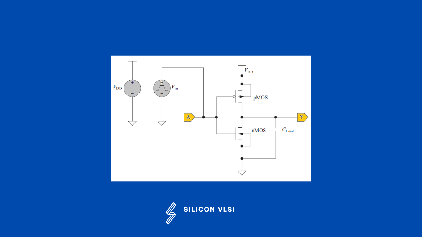
The circuit components are picked up from the symbol browser and placed in the drawing area. #
The components are then connected by drawing wires.
The input and output pins are attached to the input and output nodes.
The voltage or current source is connected to the input pins.
The capacitor is connected to the output pins to model the load seen by the pin.
The SPICE models are inserted or specified.
The circuit is then simulated.
Layout Design
The footprint of an integrated circuit, which is made up of millions of polygons, is known as the layout. Each polygon on the diagram corresponds to a particular device or circuit’s physical component. The architecture essentially depicts the various mask layers needed to build the integrated circuit. Different colors are used to depict various mask layers, let us consider the cross-sectional view of a CMOS inverter as shown in the following Figure. #
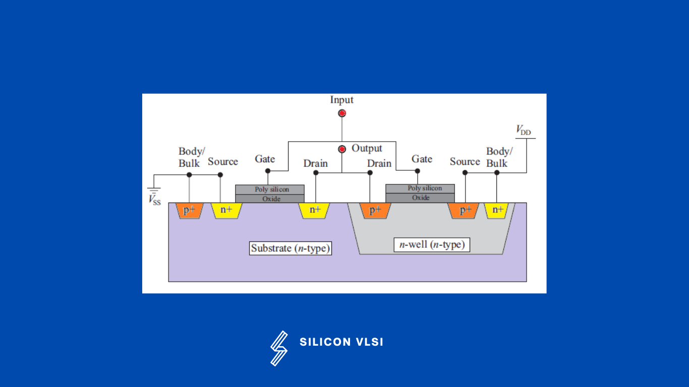
Shown in figure 1 consists of a pMOS and an nMOS transistors connected as illustrated in the schematic shown in figure 2. There are a number of different device parts as listed below.
Substrate (P substrate).
N-well (the region where pMOS is fabricated).
n+ diffusion layers (drain and source of nMOS and body/substrate contact region of pMOS).
p+ diffusion layers (drain and source of pMOS and body/substrate contact region of nMOS).
An oxide layer (gate oxide of both pMOS and nMOS).
Polysilicon layer (instead of metal gate polysilicon is used in both pMOS and nMOS).
Metal layers (to form electrical connections).
CMOS Fabrication Process Step
The fabrication process of a CMOS inverter is described as follows.
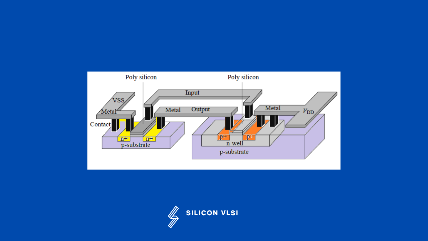
- Step 1: Create an n-well on the p-substrate to fabricate a pMOS transistor. #
- Step 2: Create n+ diffusion regions on the p-substrate to fabricate the nMOS source and drain regions.
- Step 3: Create p+ diffusion regions on the n-well region to fabricate the pMOS source and drain regions.
- Step 4: Create poly-Si layers on the oxide layers to fabricate the gate of nMOS and pMOS transistors.
- Step 5: Create contact regions required to fabricate the source/drain and substrate contact.
- Step 6: Create metal layers to fabricate the interconnect layer.
To produce the layer, each of the six processes requires a photolithography process step. Layer by layer, the layers are built up from the bottom up. As a result, planar technology is the name given to VLSI technology. Different masks are needed for the various levels.
Layer Definition in CMOS
The n-select and p-select layers are used to specify the nMOS and pMOS transistors. #
- ndiff – a combination of n-select and active
- pdiff – a combination of p-select and active
- nMOS – a combination of ndiff and poly
- pMOS – a combination of pdiff and poly
The active layer is used to specify the source/drain diffusion layers for both nMOS and pMOS.
When poly overlaps actively, it forms a MOS transistor.
An n-well layer is drawn on the p-substrate layer to create a pMOS.
Contact layers are drawn to specify the contact between poly and metal and between poly and active.
A contact between the poly and metal layer is called poly-contact
A contact between the active and metal layer is called active contact.