
List of Second-Order Effects in MOSFET:
- Subthreshold Current
- Channel length modulation(CLM)
- Body effect
- Mobility variation
- Tunneling
- Punch through
- Impact Ionization or Hot Electrons effect
Subthreshold Current:
Ids in the cutoff region is non-zero except when Vgs = 0. There is a small amount of current that will flow. As long as Vgs is non-zero for only a short period this does not cause problems. In short, the subthreshold current affects power consumption.
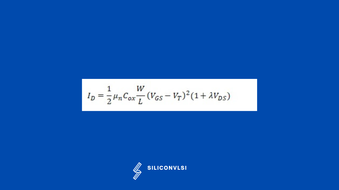
Channel Length Modulation:
The channel length decreases as Vds increase. This is not significant for large feature sizes of devices, but feature sizes are smaller for newer technologies. As the channel length decreases, the W/L ratio of the transistor increases, and it will increase the b of the transistor. The transistor does not appear as a pure current source in saturation, because the current source appears to have a finite impedance.
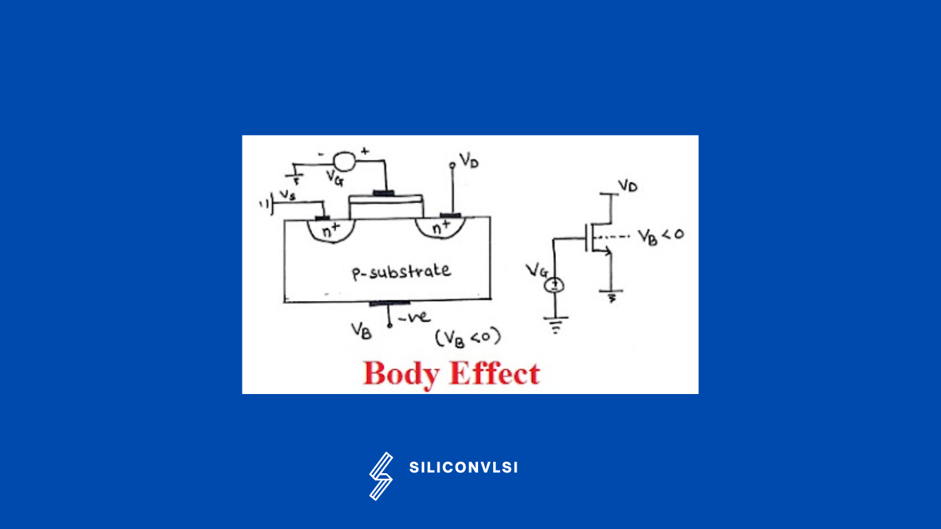
Body Effect:
Whenever there is a potential difference between the source and drain, Vt will vary, that’s called the body effect.
Mobility Variations:
Electrons have higher mobility than holes. and Mobility decreases with increasing doping concentration. Mobility decreases as temperature rises. This can affect how fast the circuits can switch from a high to low output
Tunneling: Electrons can “tunnel” through very thin oxide layers in active areas when an electric field is applied. and it may trap gate oxide, This can result in current flow between the gate and either the source or the drain in a transistor. This can actually be used to advantage when “programming” a device electronically.
Punchthrough:
When the difference between the source and drain voltages is very great, the depletion region around the drain may increase, and extend to the source. For NMOS transistors, holes are depleted around the drain, because they are attracted to the source, ground in the case of an inverter.. For PMOS transistors, electrons are depleted around the drain, because they are attracted to the source, Vdd in case of an inverter. Current then flows between the source and drain, independent of the gate voltage. This can be used to advantage in protection circuits used at the inputs to an integrated circuit.
Hot Electrons:
These electrons have very high energy and can tunnel into the gate oxide. These electrons, trapped in the gate oxide, can cause a rise in the Vt of a device. As gate lengths decrease in newer technologies, the electric field can increase. Sometimes electrons become “hot” and possess enough energy to holes (as we called as impact ionization) that are swept to the substrate, causing a substrate current. Hot electrons can also cause gate currents. This can lead to latch-up and other forms of circuit failure. Lower supply voltages help prevent hot electrons.
What are the different secondary effects observed in a short channel MOSFET?
MOSFETs with dimensions meeting those criteria are referred to as “short-channel devices.” The main second-order effects associated with short-channel devices include velocity saturation, threshold voltage variations, and hot carrier effects.