
What is Body Effect?
Whenever there is a voltage (potential) difference between the source and substrate (body), this leads to an increase or decrease in the threshold voltage of the transistor. This is called a “body effect.”
“The threshold voltage is increased or decreased due to Body effect”
In NMOS bulk and source of the transistor were tied to the ground, suppose VS = 0 and VD = 0 and VG is somewhat less than VTH so that the depletion region is formed under the gate but the inversion channel does not exist as shown in Figure below.
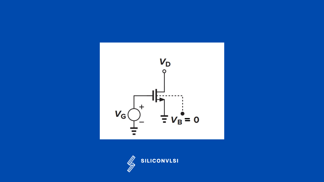
Now to understand the Body effect, let’s take three cases, here we are taking NMOS into the p substrate, the p substrate has a majority of carrier holes.
Case 1: Negative Bulk voltage.
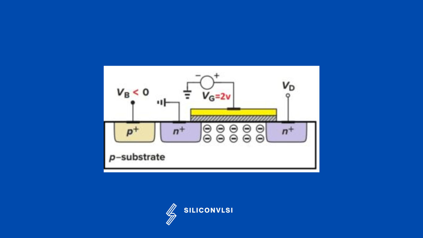
“The threshold voltage decreases with a negative bulk voltage of NMOS”
In the above figure, In Nmos let’s assume that the Gate voltage Vg is 2v and the Base terminal is tied with the negative terminal, so in this case, As Vb becomes more negative, more holes are attracted to the substrate connection, and leaving a larger negative charge behind, so the depletion region becomes wider as compare to normal.
Now we know that threshold voltage is a function of the total charge in the depletion region. Now to invert this wide depletion region, we need less threshold voltage(Vt), so due to this threshold voltage will decrease. This phenomenon is called the “body effect” or the “back-gate effect.”
Case 2: Zero Bulk voltage(no Body effect).
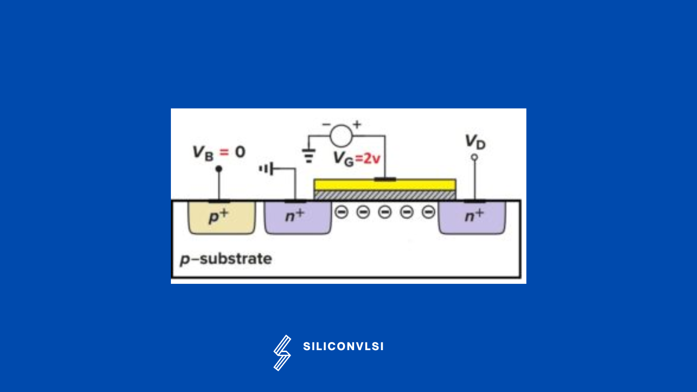
“The threshold voltage is normal with zero bulk voltage of NMOS”
In the above figure, In Nmos let’s assume that the Gate voltage Vg is 2v and the Base terminal is tied with zero. Now as the source and body terminal are tied with zero, no effect will create by the body, so the depletion region becomes normal. so due to this threshold voltage will be normal. This phenomenon we can say that there is no body effect when Source and Bulk are tied to zero terminal.
Case 3: Positive Bulk voltage.
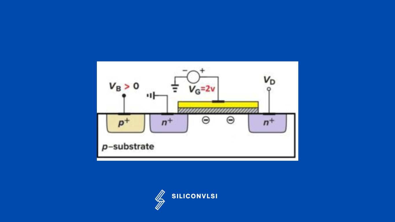
“The threshold voltage is increased with a positive bulk voltage of NMOS”
In the above figure, In Nmos let’s assume that the Gate voltage Vg is 2v and the Base terminal is tied with the positive terminal, so in this case, As Vb becomes more positive, more electrons are attracted to the substrate connection, and leaving a larger positive charge behind, so the depletion region becomes narrow as compared to normal. Now to form a channel, we need more voltage to the gate, so due to this threshold voltage will increase.
How to reduce body effect
- Provide a Strong Bulk connection
- Good Ohmic contact with the body
- Maintain Source and Body(bulk) terminal as the same potential