Understanding Stress-Induced Voiding in Metal Conductors
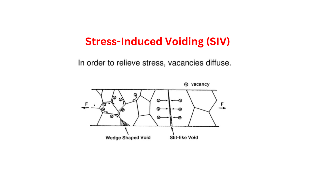
Stress-induced voiding (SIV), or stress migration, happens when metal conductor ions move due to high tensile stresses in the interconnect after certain processing steps, like passivation deposition. This migration leads to the formation of voids within the metal conductor. The root cause of these stresses is the difference in thermal expansion between the metal layer and the underlying Si-substrate, as well as between the metal and the passivation layer or intermetal dielectric.