What is Shielding in Analog Layout?
Shielding is required to protect the critical net from the outer environment. Shielding is an effective and very common technique to reduce crosstalk noise as well as delay uncertainty at the cost of the increased routing area. . In the lower technology nodes, Due to capacitive and inductive coupling effects, inserting a shield line is necessary to keep the signal integrity efficiently. The reason is the following.#
Why Shielding is necessary?
One of the most important issues that designers need to consider for the deep sub-micron (DSM) design is interconnected crosstalk noise. Because the space between two wires is typically smaller than the distance between adjacent metal layers and the wire thickness is typically more than the wire width in lower technology nodes, capacitive coupling effects between two adjacent wires are a significant design challenge in DSMs. The short-range capacitive coupling effect, which only affects two neighboring signal lines, has two harmful impacts on the integrity of the signal.#
When the signal switches on the aggressor line, noise is induced on the victim line which might result in logic malfunction. And when both the aggressor line and victim line have a signal-switching event, a change in the timing of the signal transition, called delay uncertainty, occurs in the victim lines. This all are happening because of the effect of coupling capacitance. So to avoid the coupling capacitance and to protect the victim net, we need proper shielding.
Types of Shielding in Analog Layout.
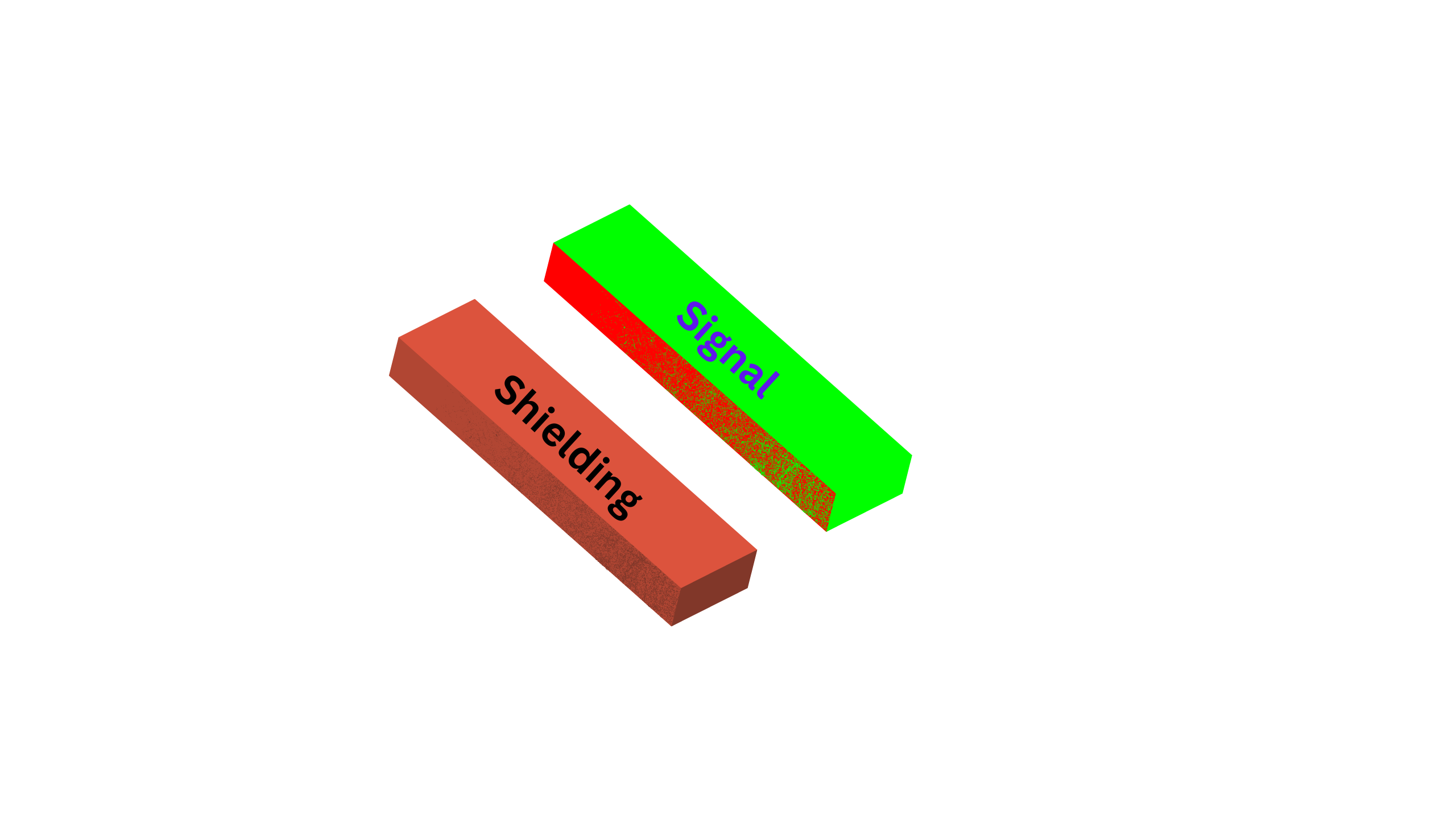
One Side Shielding
One-side shielding is a simple or normal kind of shielding. Generally, the signal, which is not more critical, we should use this kind of shielding.#

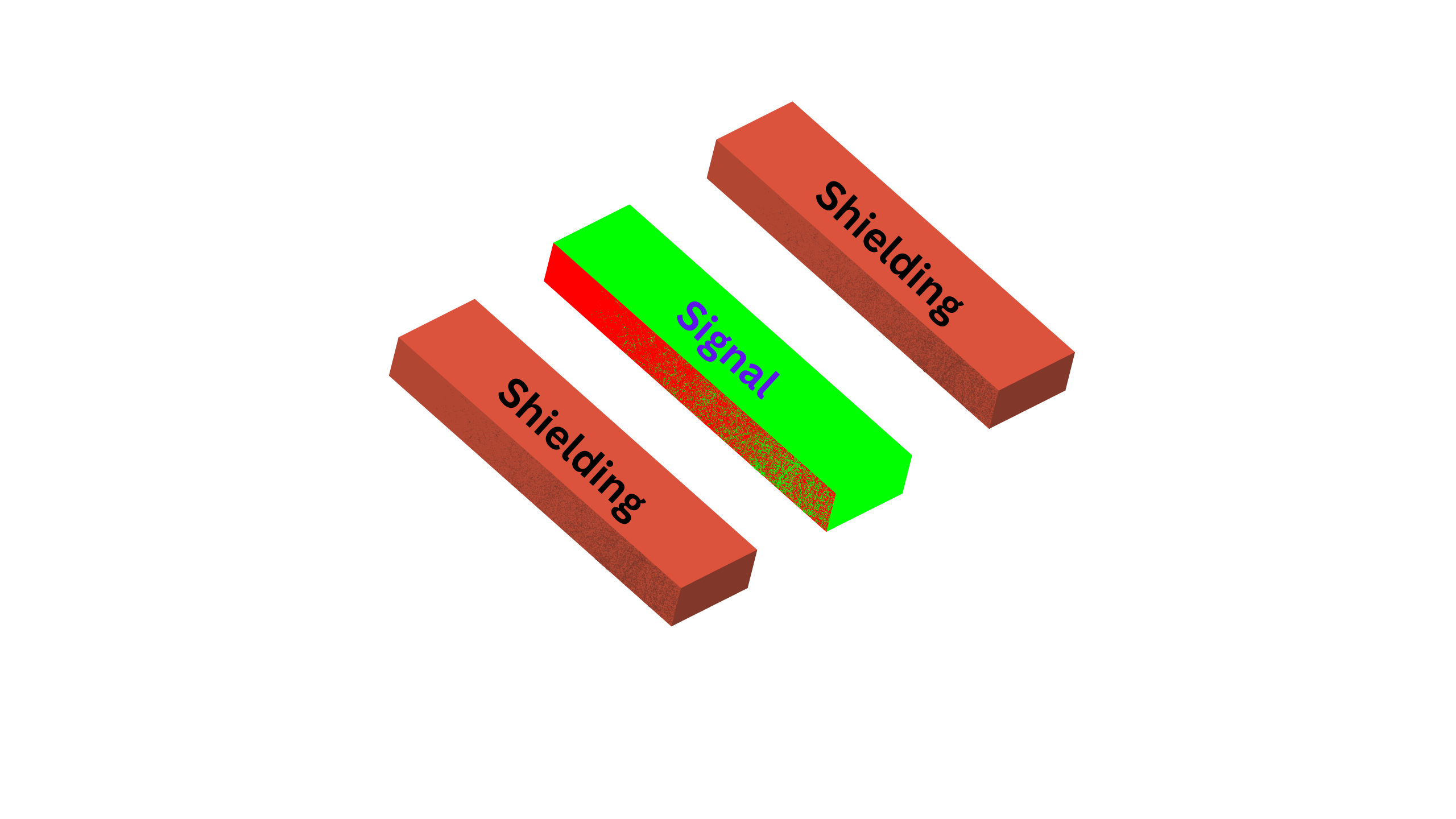
Two Side Shielding
In Analog layout, this kind of Shielding is used to protect the signal net from the clock net. We should not do shielding for the clock net, we should shield the signal net because if we shield the clock net, this net will take more time to charge and discharge, because of coupling capacitance with the shielded net, so for clock net rise and fall time will increase, and delay will increase, so to avoid that, we will not shield the clock net. The following figure is showing two-side shielding.

Coaxial Shielding
This is one of the best types of shielding in Analog layout design. It will protect the net from all sides. This means let’s assume you want to shield the metal 2 net. So as shown in the following, figure metal1 and metal3 are used as shield metals for metal2. The disadvantage of coaxial shielding is taking up more area.

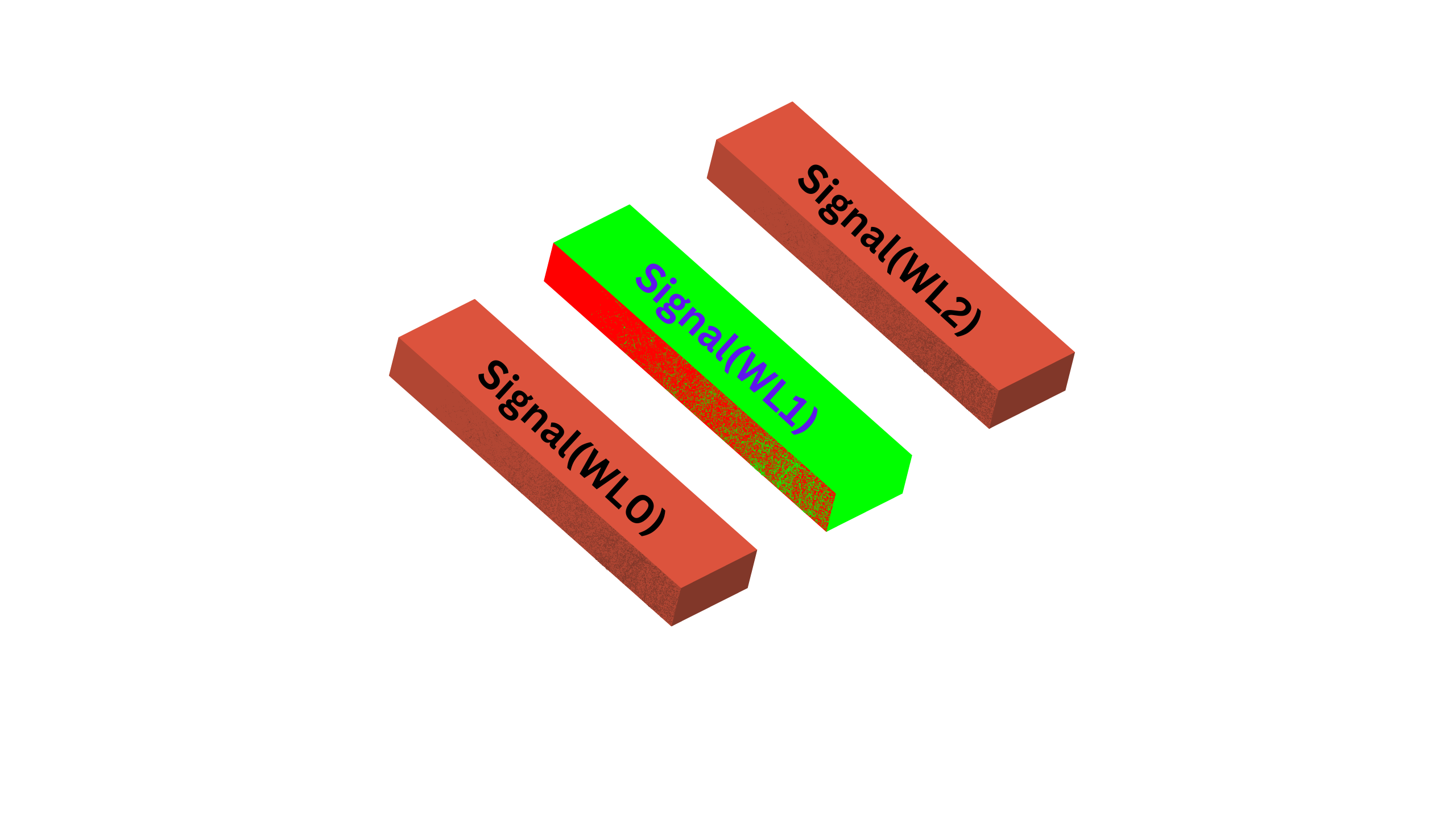
Interleave Shielding
Let’s assume You have a bunch of word lines, and from all word lines, only one-word line is active at one time. so the rest of the word line will not active. so assume that word line one is active now, so for that, word lines zero and two will act as a shied net. this is called Interleave shielding.

Where Shielding is required?
- For data path.#
- For Bias lines.
- For Reference voltages.
- In Analog Layout design.
Diasvatage of Shieding.
- It requires more area in a design.#
- Adding more Parasitic capacitance.
FAQs
What is the purpose of shielding in an analog layout?
Shielding in analog layout aims to protect sensitive analog components from external electromagnetic interference and noise, ensuring optimal signal integrity and performance.
How does shielding in analog layout improve signal integrity?
Shielding minimizes the impact of unwanted signals and external electromagnetic fields on analog components, reducing crosstalk, noise, and distortion, thereby improving signal integrity.
Are there any limitations to using shielding in an analog layout?
Yes, some limitations include increased complexity, cost implications, design trade-offs, and potential impact on the size and weight of the circuitry.
What are some best practices for effective shielding in analog layout?
Best practices include proper grounding techniques, minimizing loop area, signal isolation, and tailoring shielding techniques to specific application requirements.
How does shielding impact the overall size and weight of the design?
The use of shielding materials and techniques can increase the overall size and weight of the circuitry, which must be considered in space-constrained designs.
Please comment if You like this article.