
The growth of oxide layers impacts the silicon wafer
The growth of oxide layers during the fabrication of CMOS integrated circuits has a significant impact on the silicon wafer and is subject to distinct techniques, namely wet and dry oxide growth.
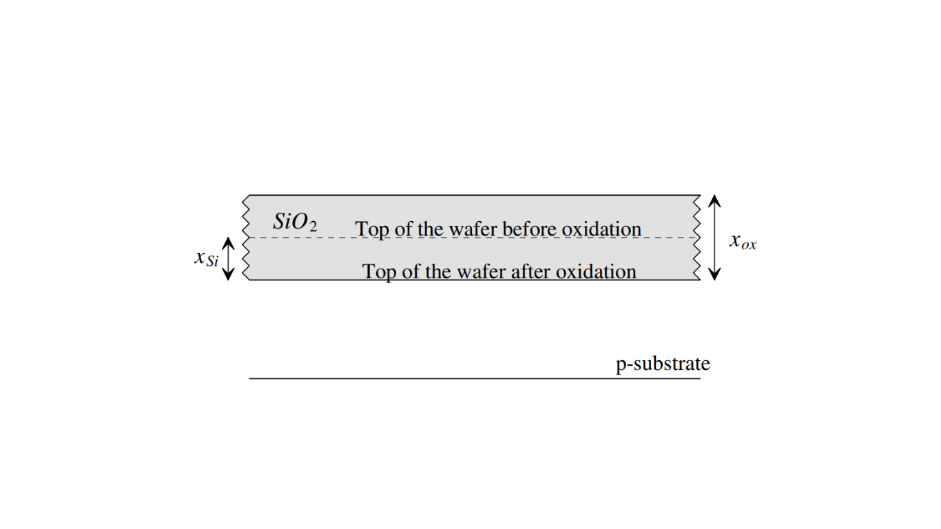
When oxide layers are grown, silicon from the wafer is consumed in the process. This consumption is visually illustrated in the following figure, where the oxide growth is seen to encroach upon the silicon substrate. The thickness of the oxide layer is directly related to the amount of silicon consumed during growth, a relationship that influences the overall dimensions of the final integrated circuit.
Wet oxide and dry oxidation
Wet oxide and dry oxide growth are two primary methods employed to create oxide layers. Wet oxide results from a reaction involving steam (H2O), while dry oxide is formed through a reaction with pure oxygen (O2). Both types are referred to as thermal oxides due to the elevated temperature required for their growth. Notably, wet oxide grows relatively quickly compared to dry oxide. However, wet oxide growth comes with a drawback – the production of hydrogen byproducts. In contrast, dry oxide growth is slower but typically yields a purer oxide layer.
Additionally, the growth rate of oxide layers increases with higher temperatures. As a consequence, both wet and dry oxide growth are used in CMOS processes, with the choice of technique depending on factors like required growth rate and desired oxide purity. The differences between wet and dry oxide growth underscore the careful control needed in semiconductor processes to achieve specific thickness and purity characteristics in the oxide layers.
What is the main advantage of wet oxide growth?
The main benefit of wet oxide growth is its faster growing time compared to dry oxide.
What is the purpose of the reticle in the CMOS patterning process?
The reticle, a single mask with larger openings than the final illuminated area, is used to project the pattern onto the wafer, generating the necessary patterns to create multiple copies of a chip.
What is the difference between a positive resist process and a negative resist process?
In a positive resist process, the illuminated areas are removed, while in a negative resist process, the areas not exposed to light are removed.