
Czochralski Process
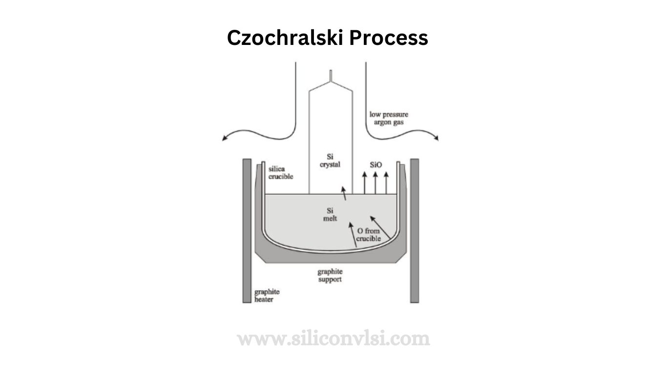
The Czochralski process is a key method for growing semiconductor-grade silicon crystals, and its principles involve careful control and technical challenges. In this process, a silica crucible containing pieces of semi-grade polycrystalline silicon is heated in an electric furnace until all the silicon melts. A small seed crystal is then introduced into the molten silicon. Controlled cooling of the melt causes silicon atoms to deposit onto the seed crystal, allowing the crystal to slowly rise and be pulled centimeter-by-centimeter from the melt. The rotation of the shaft holding the crystal ensures uniform growth. However, the high surface tension of molten silicon results in the crystal taking a cylindrical rod shape rather than the expected faceted prism.
The use of a seed crystal is crucial as it serves as a template for the deposition of additional silicon atoms. Without a seed, crystal growth would occur, but it would consist of small intergrown crystals. By using a seed, larger and more perfect crystals can be grown, suppressing undesired nucleation sites and contributing to the purity and quality of the crystal.
How to Control Czochralski process?
The Czochralski process demands meticulous control to achieve the desired crystal purity and dimensions. Automated systems regulate the temperature of the melt and the rate of crystal growth. Doped polysilicon added to the melt determines the doping concentration in the crystal. However, impurities from the silica crucible and heating elements, such as oxygen and carbon, dissolve in the molten silicon and become incorporated into the growing crystal. These impurities subtly influence the electrical properties of the resulting silicon.
Once the crystal reaches its final dimensions, it is lifted from the melt and allowed to slowly cool to room temperature, resulting in a cylindrical rod known as an ingot. Since integrated circuits are formed on the surface of a silicon crystal, the ingot is sliced into thin circular sections called wafers. A typical ingot, measuring between one and two meters in length, can provide hundreds of wafers, each capable of yielding hundreds or thousands of integrated circuits.