Close Menu
  • Analog Design
    • Latest Analog Layout Interview Questions (2025)
  • Digital Design
    • Digital Electronics Interview Question(2025)
    • Top VLSI Interview Questions
  • Physical Design
    • Physical Design Interview Questions for VLSI Engineers
  • Verilog
    • Verilog Interview Questions(2024)
  • Forum
Facebook Instagram YouTube LinkedIn WhatsApp
SiliconvlsiSiliconvlsi
Forum Questions Register in Forum Login in Forum
Facebook Instagram YouTube LinkedIn WhatsApp
  • Analog Design
    • Latest Analog Layout Interview Questions (2025)
  • Digital Design
    • Digital Electronics Interview Question(2025)
    • Top VLSI Interview Questions
  • Physical Design
    • Physical Design Interview Questions for VLSI Engineers
  • Verilog
    • Verilog Interview Questions(2024)
  • Forum
SiliconvlsiSiliconvlsi
Home»VLSI Design»Layout Design Rules – (DRC)
VLSI Design

Layout Design Rules – (DRC)

siliconvlsiBy siliconvlsiJanuary 12, 2022Updated:June 3, 2024No Comments1 Min Read
Facebook Pinterest LinkedIn Email WhatsApp
Share
Facebook Twitter LinkedIn Pinterest Email

 Layout Design Rules – (DRC)

DRC helps to check is an essential part of the physical design flow and ensures the design meets manufacturing requirements and will not result in a chip failure. Its stands for the Design Rule Check.

Design Rule Checking (DRC)

Various foundries have their own design rules for masking and They have consistent processes to convert GDS II into a real layout/final product. 

According to technology and process information, they define some set of rules which has to follow by a Physical Design Engineer while delivering GDS II.

Process design rules are the minimum allowable drawing dimensions that affect the X and Y dimensions of a layout, but not the depth or vertical dimensions. Violating a design rule could lead to a non-functional circuit or lower yield.

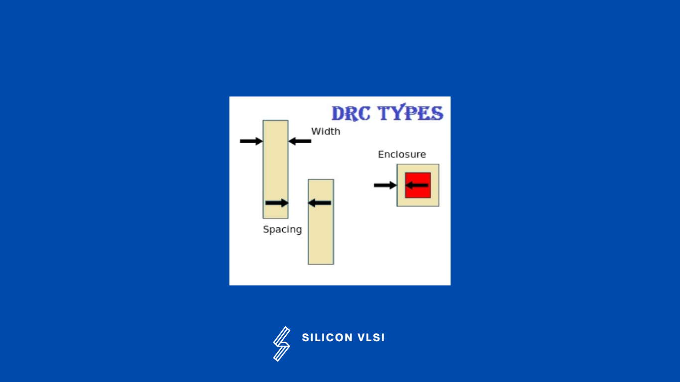
Types of Design Rule Checking

  • Minimum width 
  • Minimum spacing
  • Minimum area
  • Poly Extension from diffusion
  • Minimum width and spacing via
  • Fat wire Via keep out Enclosure
  • Different net spacing
  • Shorts violation
  • End of Line spacing
  • Metal enclosure
  • Wide metal jog
  • Misaligned Via wire
  • Center via spacing
  • Special notch spacing
  • Different net Via cut spacing
Share. Facebook Twitter Pinterest LinkedIn Tumblr Email

Related Posts

How Shielding Avoids Crosstalk Problem? What Exactly Happens There?

September 22, 2024

Navigating the Challenges of Gate Dielectric Scaling in MOS Transistors

August 1, 2024

Challenges in Modern SoC Design Verification

April 20, 2024
Leave A Reply Cancel Reply

Facebook X (Twitter) Instagram Pinterest Vimeo YouTube
  • About Us
  • Contact Us
  • Privacy Policy
© 2025 Siliconvlsi.

Type above and press Enter to search. Press Esc to cancel.