
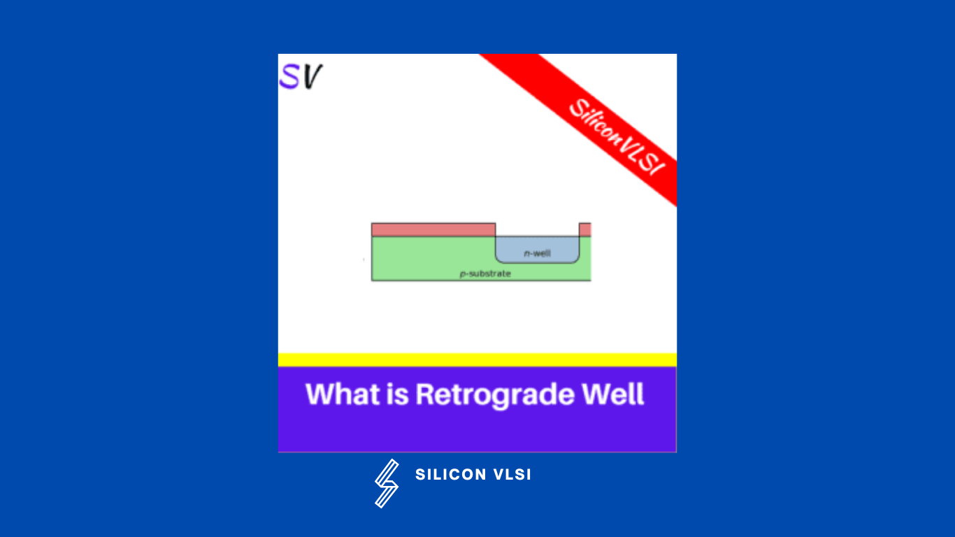
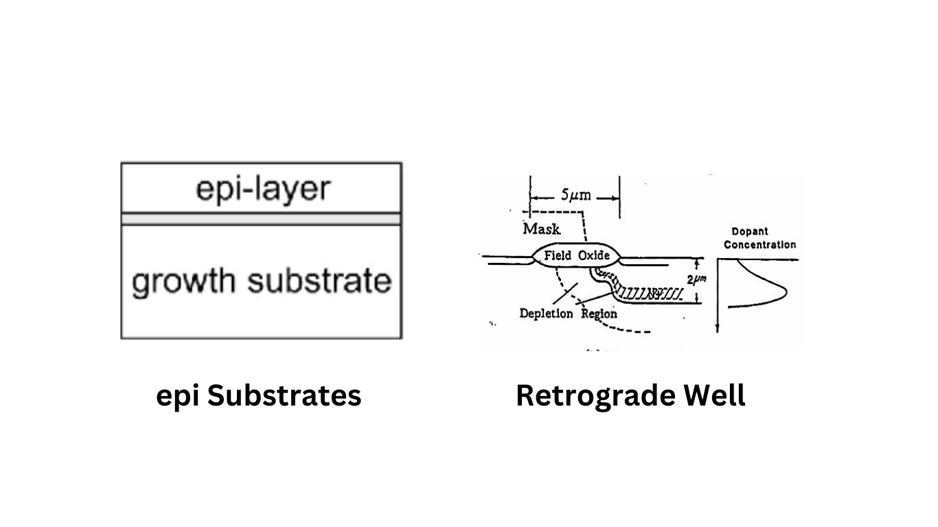
What is Retrograde Well
To increase the performance of semiconductor devices, a retrograde well is a sort of doping profile. It is made by adding impurities to a semiconductor layer in a way that results in a gradient of concentration from the layer’s surface to its bottom. #
In a retrograde well, the impurity concentration rises from low levels at the surface to higher levels near the bottom of the layer as you go deeper down the layer. Lowering carrier leakage and enhancing carrier transport qualities, generates an internal electric field that can help the device work better.
Ion Implantation
The introduction of impurities into a semiconductor material through the technique of ion implantation modifies the material’s electrical characteristics. It is an essential stage in the creation of many different kinds of semiconductor devices, including transistors, diodes, and integrated circuits. #
A beam of extremely high-energy ions is focused on the semiconductor material during the ion implantation procedure. A thin coating of contaminants is produced on the surface when the ions are implanted into the material after being accelerated to high speeds. By changing the ion beam’s energy and intensity, the depth and concentration of contaminants can be managed.
Dopants of different types, such as n-type (electron-rich) and p-type (hole-rich), are produced by ion implantation and are used to make various kinds of semiconductor devices. In order to enhance the performance of semiconductor devices, it is also utilized to build specific structures such as retrograde wells.
Ion implantation is a very precise procedure that needs specialized tools and knowledge to complete. In order to prevent contamination of the semiconductor material throughout the process, it is normally carried out in a cleanroom setting.