

Low-Power Design in VLSI: 7 Essential Techniques to Reduce Power
The goal of low-power design in VLSI is to reduce unnecessary power consumption while maintaining the required performance, functionality, and reliability of the circuit.
As transistor counts continue to increase, power has become an important design constraint. Low-power techniques are therefore considered throughout the VLSI design flow, from architecture and RTL design to physical implementation and sign-off.
A successful low-power design aims to achieve a practical balance between power, performance, area, and reliability.
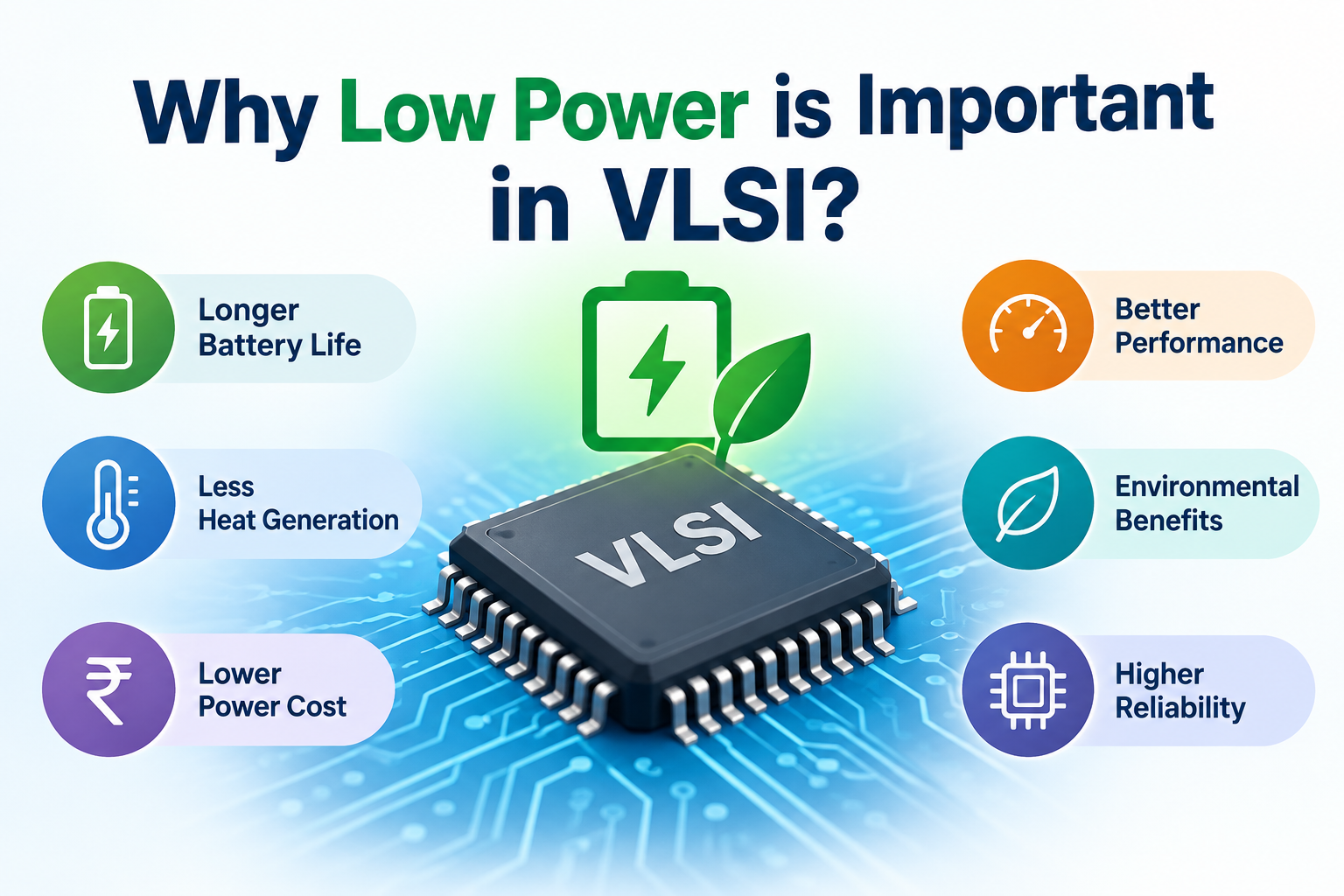
Why Is Low-Power Design Important in VLSI?
Low-power VLSI design is important for several reasons.
1. Energy Efficiency
Reducing power consumption helps electronic systems operate more efficiently.
This is particularly important for battery-powered products such as:
- Smartphones
- Smartwatches
- Wearable devices
- Wireless sensors
- Portable computers
- IoT devices
For battery-operated systems, lower power consumption can directly contribute to longer operating time between charges.
2. Heat Dissipation
Electrical power consumed by a circuit is eventually converted largely into heat.
Higher power consumption therefore increases the thermal-management requirements of a system.
Excessive temperature can affect:
- Device reliability
- Timing behavior
- Performance
- Package requirements
- System lifetime
Reducing power can help control the thermal load of an IC and its package.
3. Lower Operating Cost
For systems that operate continuously, such as servers, networking equipment, and data-center hardware, reducing power consumption can reduce energy requirements and operating costs.
At large scale, even a small reduction in power per chip can produce significant energy savings across thousands of systems.
4. Environmental Impact
Lower energy consumption can also reduce the energy required to operate electronic systems.
This is increasingly important for:
- Data centers
- Communication infrastructure
- Consumer electronics
- Automotive systems
- Large-scale computing systems
Energy efficiency has therefore become an important consideration in modern semiconductor design.
5. Better System Integration
Modern ICs integrate a very large number of transistors and functional blocks on a single chip.
Higher power density can make thermal management and package design more difficult.
Low-power techniques can help designers manage:
- Power density
- Thermal constraints
- Package limitations
- Battery requirements
- Voltage regulation requirements
6. Improved Noise and Signal Integrity
Power distribution and switching activity can introduce unwanted electrical effects such as:
- Supply droop
- Ground bounce
- Electromagnetic interference
- Simultaneous-switching noise
Reducing unnecessary switching activity and managing power delivery can help improve overall signal integrity.
However, low power does not automatically eliminate noise; power integrity and signal integrity require dedicated design and verification techniques.
What Are the Main Components of Power in VLSI?
Understanding where power comes from is the first step toward reducing it.
In CMOS circuits, total power can broadly be divided into:
Total Power ≈ Dynamic Power + Short-Circuit Power + Leakage Power
Dynamic Power
Dynamic power is associated with charging and discharging capacitances when circuit nodes switch.
A commonly used approximation is:
Pdynamic = α × C × VDD² × f
where:
- α = switching activity factor
- C = effective switched capacitance
- VDD = supply voltage
- f = switching frequency
This equation highlights an important point: power has a quadratic dependence on supply voltage in this simplified model.
Short-Circuit Power
During an input transition, both the PMOS and NMOS networks of a CMOS gate can conduct for a short period.
This creates a temporary current path between the supply and ground, producing short-circuit power.
Leakage Power
Leakage power is consumed even when a circuit is not actively switching.
Important leakage mechanisms include:
- Subthreshold leakage
- Gate leakage
- Junction leakage
- Gate-induced drain leakage (GIDL)
Leakage becomes increasingly important in advanced semiconductor technologies.
7 Important Low-Power Design Techniques in VLSI
1. Reduce Supply Voltage
Reducing VDD is one of the most effective ways to reduce dynamic power.
From:
Pdynamic = αCVDD²f
a reduction in supply voltage can produce a significant reduction in dynamic power.
However, lowering the supply voltage can also reduce:
- Noise margins
- Drive strength
- Performance
- Timing margin
Therefore, voltage scaling must be carefully balanced against performance requirements.
2. Reduce Switching Activity
Dynamic power depends on the switching activity factor α.
Reducing unnecessary transitions can therefore reduce power consumption.
Common approaches include:
- Clock gating
- Operand isolation
- Reducing unnecessary logic transitions
- Optimizing finite-state machines
- Avoiding redundant computation
Clock Gating
Clock networks can consume a significant amount of dynamic power because they switch continuously in active operating modes.
Clock gating disables the clock to an inactive block when its state does not need to change.
This prevents unnecessary switching in downstream sequential logic.
3. Reduce Capacitance
Dynamic power is proportional to the switched capacitance.
Designers can reduce capacitance through:
- Smaller cell sizes where timing permits
- Shorter interconnects
- Reduced fanout
- Buffer optimization
- Better placement
- Optimized routing
At the physical-design stage, reducing unnecessary wire length can help reduce both capacitance and power.
4. Use Multi-Voltage Design
Different blocks do not always require the same supply voltage.
A design can therefore use different voltage domains to balance power and performance.
For example:
- High-performance block → higher voltage
- Low-performance block → lower voltage
Voltage-domain crossings require appropriate techniques such as level shifters.
5. Power Gating
Power gating reduces leakage power by disconnecting an inactive block from its power supply or ground using controlled power switches.
A common implementation uses sleep transistors.
When a block enters standby mode, the power switch can be turned off, substantially reducing its leakage current.
Power gating introduces additional considerations, including:
- Wake-up time
- State retention
- IR drop
- Inrush current
- Power-switch sizing
6. Use Multi-Threshold CMOS
Different threshold-voltage cells can be used to balance performance and leakage.
For example:
- LVT cells → higher performance, generally higher leakage
- HVT cells → lower leakage, generally slower
- SVT/RVT cells → intermediate characteristics
A low-power design can use high-performance cells only where timing requires them and higher-threshold cells elsewhere.
This provides a practical trade-off between speed and leakage power.
7. Optimize Physical Design
Low-power design does not end at RTL.
Physical implementation can significantly affect power through:
- Interconnect capacitance
- Clock-tree power
- Buffering
- Cell sizing
- Routing
- Congestion
- IR drop
- Signal switching
Useful physical-design strategies include:
- Reducing unnecessary wire length
- Optimizing clock-tree structure
- Avoiding excessive buffering
- Using appropriate cell sizes
- Improving placement
- Managing high-activity nets
- Reducing unnecessary routing capacitance
Power analysis should therefore be performed throughout implementation rather than only at the end.
Low-Power Design at Different VLSI Levels
Low-power techniques can be applied at several stages.
| Design Level | Examples of Low-Power Techniques |
|---|---|
| Architecture | Parallelism optimization, power-aware architecture |
| RTL | Clock gating, operand isolation |
| Logic synthesis | Logic optimization, cell selection |
| Circuit | Voltage scaling, transistor sizing |
| Physical Design | Placement, routing, clock optimization |
| Sign-off | Power analysis, IR-drop analysis, thermal analysis |
The earlier power is considered in the design process, the more opportunities designers have to reduce it.
Dynamic Power vs Leakage Power
| Feature | Dynamic Power | Leakage Power |
|---|---|---|
| Main cause | Switching activity | Current when devices are not actively switching |
| Depends on | Activity, capacitance, voltage, frequency | Device/process conditions and transistor state |
| Important technique | Clock gating, voltage scaling | Power gating, high-VT cells |
| Voltage dependence | Strong | Also voltage-dependent, but through different mechanisms |
| Physical design impact | Significant | Significant |
Both components need to be considered when optimizing modern VLSI systems.
Important Trade-Offs in Low-Power Design
Reducing power is not simply a matter of minimizing every circuit parameter.
For example:
Lower VDD → Lower dynamic power but potentially lower performance
Higher VTH → Lower leakage but potentially slower operation
Smaller cells → Lower capacitance but potentially lower drive strength
Power gating → Lower standby leakage but additional area and wake-up considerations
Therefore, practical low-power design is an optimization problem involving:
Power + Performance + Area + Reliability
Low-Power Design Flow
A simplified low-power VLSI design flow can be represented as:
Architecture → RTL → Synthesis → Floorplanning → Placement → CTS → Routing → Extraction → Power Analysis → Sign-Off
Power should be estimated and optimized at multiple stages.
For example, after placement and routing, extracted parasitic capacitances can provide a more realistic basis for power estimation than early-stage estimates.
Common Low-Power Design Mistakes
Ignoring Leakage Power
Dynamic power is not the only source of power consumption. Leakage can become a major contributor, particularly in advanced technologies and standby modes.
Reducing Voltage Without Checking Timing
Lower VDD can reduce dynamic power but may also reduce transistor drive strength and increase delay.
Excessive Clock Gating
Clock gating can save power, but poorly designed clock-gating structures can introduce timing, area, test, and implementation challenges.
Ignoring Physical Design
A logically optimized circuit can still consume significant power because of long wires, large capacitance, excessive buffering, or an inefficient clock network.
Optimizing Power Without Considering Reliability
Power reduction techniques must be checked against timing, IR drop, electromigration, thermal behavior, and other reliability requirements.
Frequently Asked Questions
What is low-power design in VLSI?
Low-power design in VLSI is the process of reducing dynamic, short-circuit, and leakage power while maintaining the required performance, functionality, area, and reliability.
What is the most effective way to reduce dynamic power?
Supply-voltage reduction can be highly effective because dynamic power has a quadratic dependence on VDD in the simplified CMOS power equation. However, voltage scaling must be balanced against timing and noise-margin requirements.
How does clock gating reduce power?
Clock gating prevents the clock from switching in inactive blocks, reducing unnecessary transitions in sequential logic and associated clock-network power.
What is power gating?
Power gating disconnects an inactive circuit block from its supply or ground through controlled power switches, reducing standby leakage.
How does multi-VT help reduce power?
Multi-threshold CMOS allows designers to use high-VT cells in non-critical paths to reduce leakage while using lower-VT cells where higher performance is required.
Is low-power design only an RTL problem?
No. Power is influenced by architecture, RTL, synthesis, cell selection, placement, routing, clock distribution, and operating conditions. Low-power optimization should therefore continue throughout the VLSI design flow.
Conclusion
Low-power design in VLSI is essential for modern semiconductor systems because power affects battery life, thermal management, performance, reliability, packaging, and operating cost.
The main power components are dynamic power, short-circuit power, and leakage power. Designers can reduce them through techniques such as voltage scaling, clock gating, capacitance reduction, multi-voltage design, power gating, multi-VT cell selection, and physical-design optimization.
The most effective approach is not to rely on a single technique. Instead, power should be considered from the architecture level through physical implementation and sign-off, while continuously balancing power, performance, area, and reliability.