

Deep Sub-Micron (DSM) in VLSI: 7 Essential Effects and Challenges
What Is Deep Sub-Micron (DSM)?
Deep Sub-Micron (DSM) technology refers to semiconductor technologies where transistor and interconnect dimensions are very small. Traditionally, the term was commonly associated with feature sizes below 0.18 µm (180 nm).
As VLSI technology scales down, transistor dimensions become smaller and transistor density increases. Scaling also affects parameters such as oxide thickness, supply voltage, interconnect dimensions, and device capacitances.
Different scaling approaches, including constant-field scaling and constant-voltage scaling, have been studied to understand how device parameters change as dimensions are reduced.
Deep Sub-Micron technology enables a much larger number of transistors to be integrated onto a single chip[1]. However, continued scaling also makes several physical effects more important.
The major DSM concerns include:
- Interconnect delay
- Crosstalk and signal integrity
- Power consumption
- Reliability
- Increasing interconnect resistance and capacitance
- Higher current-density concerns
- More difficult timing and physical-design optimization
These effects mean that modern VLSI design cannot focus only on transistor performance. Interconnects and physical implementation also have a major influence on overall chip performance.
1. Interconnect Delay in DSM
One of the important effects of DSM technology is the increasing importance of interconnect delay.
As transistor switching becomes faster, the delay associated with wires can become a significant part of the total path delay. Wire resistance and capacitance determine how quickly a signal can propagate and settle.
A simplified RC relationship is:
Delay ∝ R × C
where:
- R = interconnect resistance
- C = interconnect capacitance
As interconnect dimensions shrink, resistance can increase significantly because the available conductor cross-sectional area becomes smaller.
The original article gives an illustrative comparison of approximately 15 ps for a 1 mm wire at 0.5 µm versus 340 ps at 0.1 µm. These values should be treated as technology-dependent examples rather than universal wire-delay values.
How Can Interconnect Delay Be Reduced?
Several approaches can be used to manage interconnect delay:
- Use lower-resistivity conductors such as copper.
- Optimize wire dimensions.
- Use appropriate upper metal layers for long critical nets.
- Reduce unnecessary wire length.
- Use low-k dielectric materials to reduce capacitance.
- Insert repeaters or buffers where appropriate.
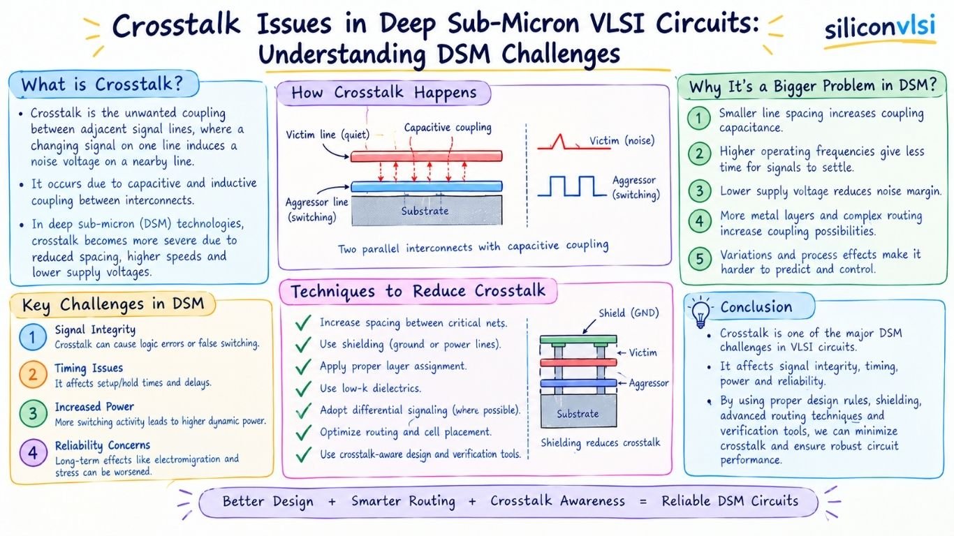
2. Crosstalk Noise in Deep Sub-Micron VLSI
As interconnects become closely spaced, coupling capacitance between neighboring wires becomes increasingly important.
When one signal switches, part of its transition can couple into a nearby signal. The switching wire is commonly called the aggressor, while the affected wire is called the victim.
This interaction can produce:
- Crosstalk noise
- Additional delay
- Timing uncertainty
- Signal-integrity problems
High-density routing and closely spaced interconnects can increase coupling effects. Therefore, accurate physical-design rules and appropriate routing strategies are important in DSM technologies.
How Can Crosstalk Be Reduced?
Common approaches include:
- Increasing spacing between critical nets.
- Reducing parallel run length.
- Using shielding where appropriate.
- Optimizing routing layers.
- Controlling transition times.
- Buffering critical nets.
- Applying technology-specific design rules.
3. Power Consumption in DSM
Power is another important consideration as VLSI technology scales.
A commonly used approximation for CMOS dynamic power is:
Pdynamic = α × C × VDD² × f
where:
- α = switching activity
- C = effective capacitance
- VDD = supply voltage
- f = operating frequency
Reducing supply voltage can significantly reduce dynamic power because dynamic power has a quadratic dependence on VDD.
However, voltage scaling also introduces trade-offs involving performance, noise margins, leakage, and device operation.
Static and Leakage Power
As transistor dimensions and threshold-voltage strategies evolve, leakage power can become an important part of total chip power.
Therefore, DSM designs often require techniques such as:
- Multi-threshold-voltage design
- Power gating
- Clock gating
- Voltage scaling
- Leakage-aware cell selection
- Power-aware physical design
4. Reliability Challenges
Scaling also makes certain reliability concerns more important.
One example is electromigration, where high current density can gradually move metal atoms and eventually affect interconnect reliability.
Other concerns can include:
- Increased current density
- Self-heating
- Voltage-related reliability
- Time-dependent dielectric degradation
- Process variation
- Signal-integrity effects
Therefore, reliability checks have become an important part of modern VLSI signoff.
5. Resistance and Capacitance Become More Important
A smaller geometry does not automatically mean that every electrical parameter improves.
For interconnects, reducing conductor dimensions can increase resistance. At the same time, neighboring wires can have significant coupling capacitance.
The overall behavior therefore depends on the combined effects of:
Resistance + Capacitance + Inductance + Coupling
For many on-chip interconnects, RC effects dominate, although inductive effects can become relevant for particular high-speed or long interconnect structures.
6. Materials Used to Manage DSM Effects
Material selection is another important part of advanced interconnect technology.
Copper Interconnects
Copper has lower resistivity than aluminum, which can help reduce interconnect resistance.
Copper also has good electromigration characteristics compared with traditional aluminum interconnect approaches, although reliability depends on the complete process and interconnect structure.
Low-k Dielectrics
Using dielectric materials with a lower dielectric constant can reduce parasitic capacitance between interconnects.
Lower capacitance can help reduce:
- RC delay
- Dynamic power
- Crosstalk-related coupling
However, advanced low-k materials can introduce mechanical and integration challenges.
7. DSM and Physical Design
Deep Sub-Micron technology has made physical design increasingly important.
Designers must consider not only whether the logic is functionally correct, but also whether the physical implementation satisfies:
- Timing requirements
- Signal-integrity requirements
- Power constraints
- Electromigration limits
- Design rules
- Density requirements
- Manufacturability requirements
This is why physical-design stages such as placement, clock-tree synthesis, routing, timing analysis, DRC, and signal-integrity analysis are closely connected to DSM challenges.
Deep Sub-Micron Effects at a Glance
| DSM Effect | Main Concern | Typical Design Response |
|---|---|---|
| Interconnect delay | Higher wire RC delay | Buffering, wider/upper metals, shorter routes |
| Crosstalk | Coupling between nets | Spacing, shielding, routing optimization |
| Power | Dynamic and leakage power | Voltage scaling, clock/power gating |
| Reliability | Current density and aging | EM and reliability analysis |
| Resistance | Smaller conductor dimensions | Better metals and optimized routing |
| Capacitance | Coupling and parasitic capacitance | Low-k materials and spacing |
| Process variation | Device and timing variation | Variation-aware design and signoff |
Deep Sub-Micron vs Traditional Scaling
The major change introduced by DSM technology is that transistor scaling alone is no longer sufficient to describe chip performance.
In earlier technologies, reducing transistor dimensions could provide substantial improvements in speed and density. With increasingly small geometries, however, interconnect resistance, capacitance, coupling, leakage, variation, and reliability become increasingly important.
As a result, successful VLSI design requires device-level, circuit-level, and physical-design optimization together.
Frequently Asked Questions
What does DSM mean in VLSI?
DSM stands for Deep Sub-Micron. Traditionally, it referred to technologies with feature sizes below approximately 0.18 µm, although terminology has evolved as semiconductor technology has progressed.
Why does interconnect delay become important in DSM?
As transistor switching becomes faster and wires become smaller, interconnect resistance and capacitance can contribute significantly to overall path delay.
What is crosstalk in DSM technology?
Crosstalk occurs when electrical coupling between nearby interconnects causes unwanted voltage or timing effects on a victim net.
Does scaling always reduce power?
No. Voltage scaling can reduce dynamic power, but leakage, switching activity, capacitance, frequency, and other design factors also affect total power.
Why is copper used in advanced interconnects?
Copper has lower resistivity than aluminum and can help reduce interconnect resistance. Its integration also requires appropriate process and barrier technologies.
Conclusion
Deep Sub-Micron (DSM) technology has enabled higher transistor density and continued VLSI scaling, but it has also introduced increasingly important physical-design challenges.
Interconnect delay, crosstalk, power consumption, current density, reliability, parasitic capacitance, and process variation all need to be considered when designing advanced chips.
For this reason, DSM design requires close coordination between RTL, circuit design, physical design, timing analysis, signal integrity, power analysis, and manufacturing considerations.
References
- R. Joshi and K. Roy, “Design of deep sub-micron CMOS circuits”, in 16th International Conference on VLSI Design, 2003. Proceedings., IEEE Comput. Soc, pp. 15–16. doi: 10.1109/icvd.2003.1183105.