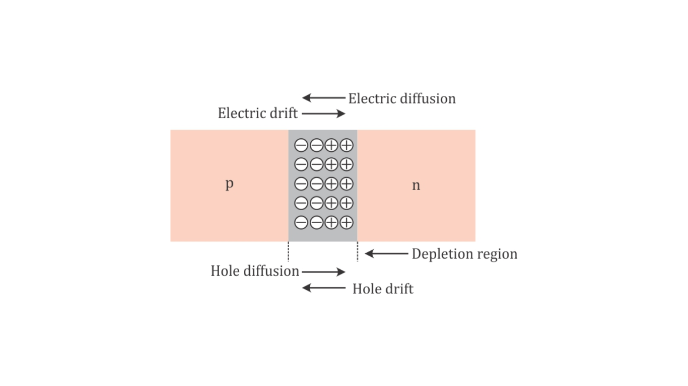
Close Menu
  • Analog Design
    • Latest Analog Layout Interview Questions (2025)
  • Digital Design
    • Digital Electronics Interview Question(2025)
    • Top VLSI Interview Questions
  • Physical Design
    • Physical Design Interview Questions for VLSI Engineers
  • Verilog
    • Verilog Interview Questions(2024)
  • Forum
Facebook Instagram YouTube LinkedIn WhatsApp
SiliconvlsiSiliconvlsi
Ask Questions Register in Forum Login in Forum
Facebook Instagram YouTube LinkedIn WhatsApp
  • Analog Design
    • Latest Analog Layout Interview Questions (2025)
  • Digital Design
    • Digital Electronics Interview Question(2025)
    • Top VLSI Interview Questions
  • Physical Design
    • Physical Design Interview Questions for VLSI Engineers
  • Verilog
    • Verilog Interview Questions(2024)
  • Forum
SiliconvlsiSiliconvlsi
Home»VLSI Design»Depletion Region: Definition
VLSI Design

Depletion Region: Definition

siliconvlsiBy siliconvlsiJuly 11, 2023Updated:September 6, 2024No Comments2 Mins Read
Facebook Pinterest LinkedIn Email WhatsApp
Share
Facebook Twitter LinkedIn Pinterest Email

Depletion Region

I find that the layer where the flow of charges slows down is called the Depletion Region. This region acts as a barrier to stop electrons from moving from the n-side to the p-side of the semiconductor diode.

We should understand that this barrier is crucial for the diode’s function, as it controls the flow of current through the device. You might notice that without this Depletion Region, the semiconductor diode wouldn’t work properly, as it wouldn’t effectively control the direction of current flow.

The junction between the p-type and n-type materials behaves differently from each side of the material alone when they are kept in contact with one another. At the junction, electrons and holes are in close proximity to one another. Coulomb’s law states that a force exists between the positive holes and the negative electrons. A few n-type electrons diffuse through the p-n junction during its formation, combining with the holes on the p-side to generate negative ions while leaving behind positive ions on the n-side. As a result, the depletion layer is created, acting as a barrier to prevent additional electron transport from the n area to the p region.

What is a Depletion Region


PN Junction Depletion Zone Semiconductor Junctions
Share. Facebook Twitter Pinterest LinkedIn Tumblr Email

Related Posts

How Shielding Avoids Crosstalk Problem? What Exactly Happens There?

September 22, 2024

Navigating the Challenges of Gate Dielectric Scaling in MOS Transistors

August 1, 2024

Challenges in Modern SoC Design Verification

April 20, 2024
Leave A Reply Cancel Reply

Facebook X (Twitter) Instagram Pinterest Vimeo YouTube
  • About Us
  • Contact Us
  • Privacy Policy
© 2025 Siliconvlsi.

Type above and press Enter to search. Press Esc to cancel.