
Higher nodes and Lower nodes in VLSI
The technology shrinking is going on for decades. since then so many changes came into the VLSI industry. For technologies <28nm and above the body, the terminal is there and the technology is CMOS technology but below 28nm, we are using FINFET technology. As we go for lower nodes, lithography challenges will increase.
- We are using double patterning in the Lower technology node, while in higher technology, it is not required.
- The processing complexities of the same are increasing in lower technology.
- In lower technology, the cost of fabricating will increase.
- As technology is shrinking, the net parasitic started dominating, and fabrication of the fine features is difficult, when the process used for the lithography is unable to produce small features like metal pitches, complex processing steps like double patterning has to be used. Also, the power supply voltage is reduced, causing it more difficult to keep the devices working, especially when there are long metal lines for power distribution.
- A smaller line width will consume less power. Resistance is heat and in the case of a device running on battery power, the less heat you produce the lower the current draw.
-
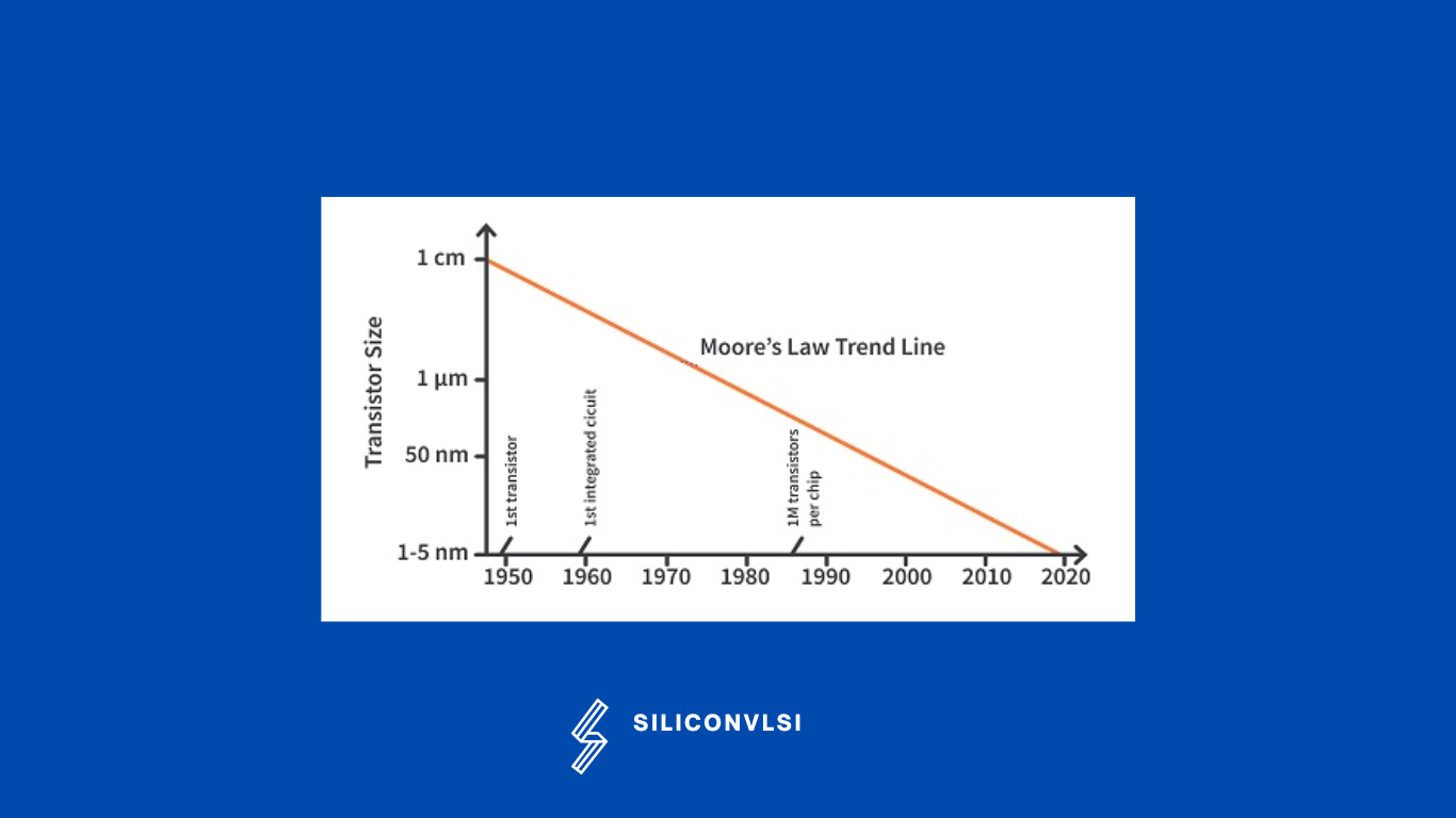
Moore’s Law Trend Line
What is the difference between a 3nm and a 5nm processor?
The main difference is the 3nm processor is smaller than the 5mn processor. In 3nm processor will consume less power and will produce less heat as compared to the 5 nm chipset. and due to this, the 3nm processor will be faster as it will be less affected by heat as compared to the 5 nm. Another difference is the price. you will get the 5mn processor cheaper as compared to the 3mn. You will take the PO(gate) connection over OD(Diffusion) in 3 nm, I think it’s the biggest advantage of 3nm technology, However in Analog layout, the designer prefers to take gate control outside of OD(Diffusion) in 3nm technology.