
Close Menu
  • Analog Design
    • Latest Analog Layout Interview Questions
  • Digital Design
    • Digital Electronics Interview Question
    • Top VLSI Interview Questions
  • Physical Design
    • Physical Design Interview Questions for VLSI Engineers
  • Verilog
    • Verilog Interview Questions(2026)
  • Forum
  • Calculators
    • Asynchronous FIFO Depth Calculator
    • Clock Skew and Clock Jitter Calculator
    • Setup Time Calculator
Facebook Instagram YouTube LinkedIn WhatsApp
SiliconvlsiSiliconvlsi
Ask Questions Register in Forum Login in Forum
Facebook Instagram YouTube LinkedIn WhatsApp
  • Analog Design
    • Latest Analog Layout Interview Questions
  • Digital Design
    • Digital Electronics Interview Question
    • Top VLSI Interview Questions
  • Physical Design
    • Physical Design Interview Questions for VLSI Engineers
  • Verilog
    • Verilog Interview Questions(2026)
  • Forum
  • Calculators
    • Asynchronous FIFO Depth Calculator
    • Clock Skew and Clock Jitter Calculator
    • Setup Time Calculator
SiliconvlsiSiliconvlsi
Home ยป How do I get Vias resistance information within a new process?
Digital Design

How do I get Vias resistance information within a new process?

siliconvlsiBy siliconvlsiApril 6, 2024Updated:November 25, 2025No Comments2 Mins Read
Facebook Pinterest LinkedIn Email WhatsApp
Share
Facebook Twitter LinkedIn Pinterest Email

Table of Contents

Toggle
  • Vias resistance information
      • Consult Process Documentation
      • Check PDK Documentation
      • Use Design Tools

Vias resistance information

To obtain information about the resistance of vias within a new process, you typically need access to the process design kit (PDK) provided by the semiconductor foundry or fabrication facility. Here’s a general guide on how you can retrieve via resistance information within a new process:
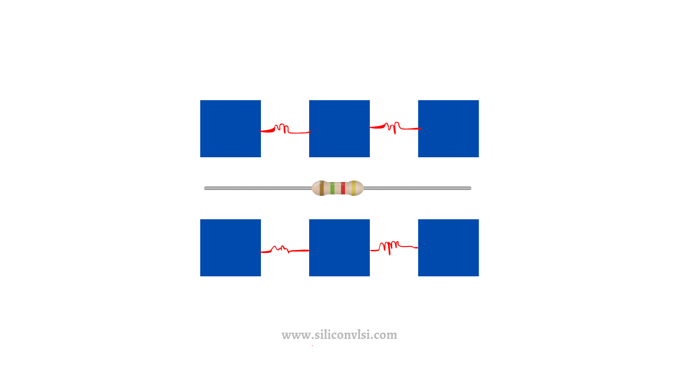
Vias resistance

Consult Process Documentation

Start by reviewing the documentation provided in the process design kit (PDK) for the new process. This documentation should include details about the materials, layers, and dimensions used in the fabrication process, which can help you understand the properties of vias and their expected resistance.

Check PDK Documentation

Look specifically for information related to via resistance or via properties in the PDK documentation. This may include specifications such as via dimensions (width, height, aspect ratio), via material composition, and any resistance models provided by the foundry.

Use Design Tools

Utilize electronic design automation (EDA) tools or layout editors provided within the PDK to create test structures or dummy layouts that include vias. You can then perform simulations or extract parasitic parameters using the tools to estimate via resistance based on the layout and process parameters.

By following these steps and leveraging the resources provided in the process design kit (PDK), collaborating with foundry support, and conducting your own experiments and simulations, you can gather valuable information about via resistance within a new semiconductor process.

Share. Facebook Twitter Pinterest LinkedIn Tumblr Email

Related Posts

Voltage-Aware DRC: 7 Essential Concepts for Reliable Signoff

September 14, 2026

Difference Between Clipper and Clamper

June 22, 2025

What is difference Between RAM Bandwidth and Clock Speed

December 1, 2024
Leave A Reply Cancel Reply

Facebook X (Twitter) Instagram Pinterest Vimeo YouTube
  • About Us
  • Contact Us
  • Privacy Policy
© 2026 Siliconvlsi.

Type above and press Enter to search. Press Esc to cancel.