Close Menu
  • Analog Design
    • Latest Analog Layout Interview Questions (2025)
  • Digital Design
    • Digital Electronics Interview Question(2025)
    • Top VLSI Interview Questions
  • Physical Design
    • Physical Design Interview Questions for VLSI Engineers
  • Verilog
    • Verilog Interview Questions(2024)
  • Forum
Facebook Instagram YouTube LinkedIn WhatsApp
SiliconvlsiSiliconvlsi
Forum Questions Register in Forum Login in Forum
Facebook Instagram YouTube LinkedIn WhatsApp
  • Analog Design
    • Latest Analog Layout Interview Questions (2025)
  • Digital Design
    • Digital Electronics Interview Question(2025)
    • Top VLSI Interview Questions
  • Physical Design
    • Physical Design Interview Questions for VLSI Engineers
  • Verilog
    • Verilog Interview Questions(2024)
  • Forum
SiliconvlsiSiliconvlsi
Home»VLSI Design»NMOS Inverter in VLSI
VLSI Design

NMOS Inverter in VLSI

siliconvlsiBy siliconvlsiJuly 27, 2023Updated:July 28, 2024No Comments2 Mins Read
Facebook Pinterest LinkedIn Email WhatsApp
Share
Facebook Twitter LinkedIn Pinterest Email

NMOS Inverter

The MOSFET (Metal-Oxide-Semiconductor Field-Effect Transistor) is a versatile electronic component widely used as a switch in various electronic applications. It offers advantages over mechanical switches in terms of speed and reliability. In this context, the MOSFET switch is also known as an inverter.

NMOS Inverter Circuit

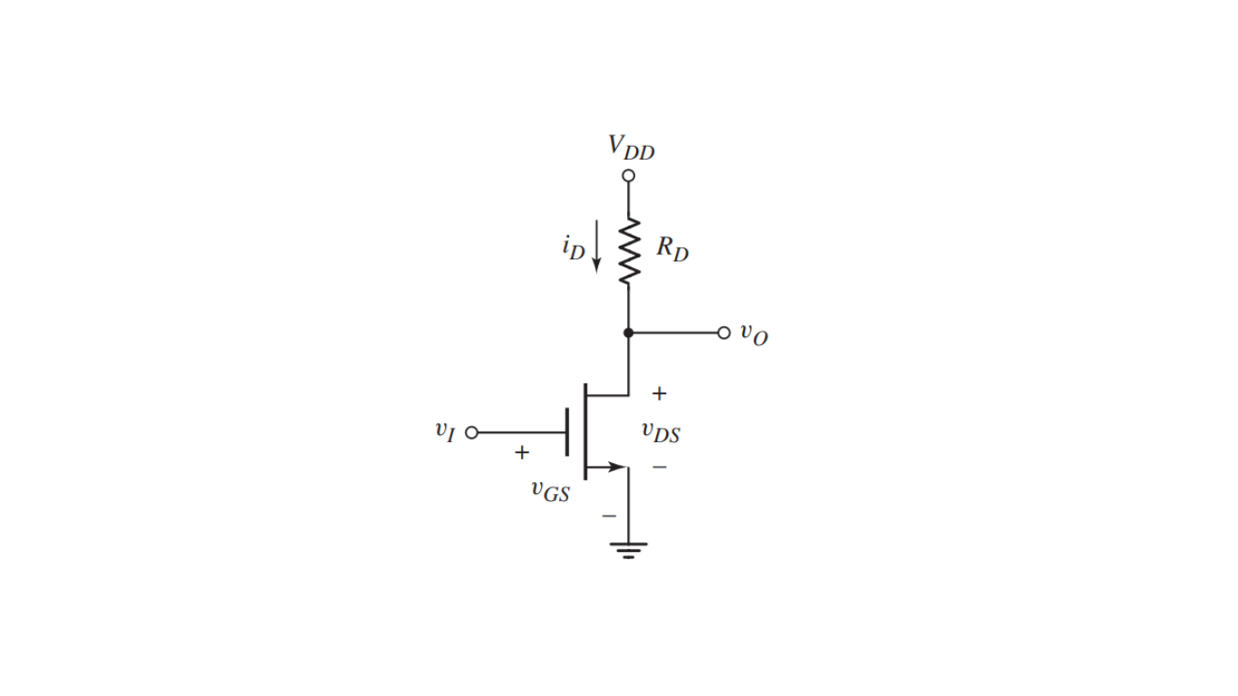
Understanding the NMOS Inverter Circuit

The figure illustrates the circuit of an n-channel enhancement-mode MOSFET inverter. When the input voltage, vI, is less than the threshold voltage, VT_N, the transistor is in cutoff mode, and the drain current, iD, is zero. Consequently, there is no voltage drop across RD (drain resistor), and the output voltage, vO, becomes equal to VDD (supply voltage). Since there is no drain current (iD = 0), no power is dissipated in the transistor.

When the Transistor Turns On

On the other hand, when the input voltage, vI, is greater than the threshold voltage, VT_N, the transistor is turned on, initially biased in the saturation region, as vDS (drain-to-source voltage) is greater than vGS – VT_N. As the input voltage continues to increase, the drain-to-source voltage decreases, and the transistor eventually moves into the non-saturation region.

Maximum and Minimum Values

At vI = VDD, the transistor is biased in the non-saturation region, vO reaches its minimum value, and the drain current, iD, reaches its maximum value. The expressions for the current and voltage are as follows:

iD = Kn * (2(vI – VT_N) * vO – vO^2)

vO = VDD – (iD * RD)

where vO represents vDS and vI represents vGS.


Share. Facebook Twitter Pinterest LinkedIn Tumblr Email

Related Posts

How Shielding Avoids Crosstalk Problem? What Exactly Happens There?

September 22, 2024

Navigating the Challenges of Gate Dielectric Scaling in MOS Transistors

August 1, 2024

Challenges in Modern SoC Design Verification

April 20, 2024
Leave A Reply Cancel Reply

Facebook X (Twitter) Instagram Pinterest Vimeo YouTube
  • About Us
  • Contact Us
  • Privacy Policy
© 2025 Siliconvlsi.

Type above and press Enter to search. Press Esc to cancel.